Introduction
Patch antenna printed circuit boards (PCBs) are among the most common pieces of radio frequency (RF) hardware that exist in modern systems today.
Wireless communications, automotive radar, and aerospace/defense systems rely heavily on these structures for transmitting and receiving electromagnetic energy.
Since these structures are produced at scale, it’s critical for RF/Microwave Engineers to understand how to characterize and test them accurately and efficiently.
The Problem
When a device radiates an electromagnetic field in a non-free-space environment, the field can reflect off nearby structures, propagate back toward the device, and distort the true measured performance of the radiating PCB.
To fully characterize all the antenna parameters, such as gain, sidelobes, and polarization, measurements must be performed in an anechoic chamber that closely approximates free-space conditions.
This is typically achieved by lining the walls of a sufficiently large enclosure with RF absorbing material (RAM).
These chambers are very expensive, time-consuming, and difficult to manage and maintain, making them impractical for many production environments.
The Solution
For build-to-print PCB manufacturers, full antenna characteristic measurements are often overkill unless explicitly required by contract.
In many defense-related cases, customers may restrict access to full antenna performance data.
A practical alternative is to use RF absorber material in conjunction with S11 measurements to validate antenna performance.
This approach involves placing the radiating side of the antenna face down to the absorber while probing the antenna’s feed structure from above — typically through a connector interface or probe.
The absorber will provide a first-order approximation of free-space while the S11 measurement verifies the antenna is well-matched and operating in the intended frequency band.
Let’s walk through a practical example of choosing RF absorbent material, configuring the full RAM/vector network analyzer setup, and how to troubleshoot poor S11 measurements.
The device under test in question is a 2.4 GHz (SubMiniature version A connector) probe-fed microstrip patch antenna. The band of interest is 1.4 GHz – 3.4 GHz.
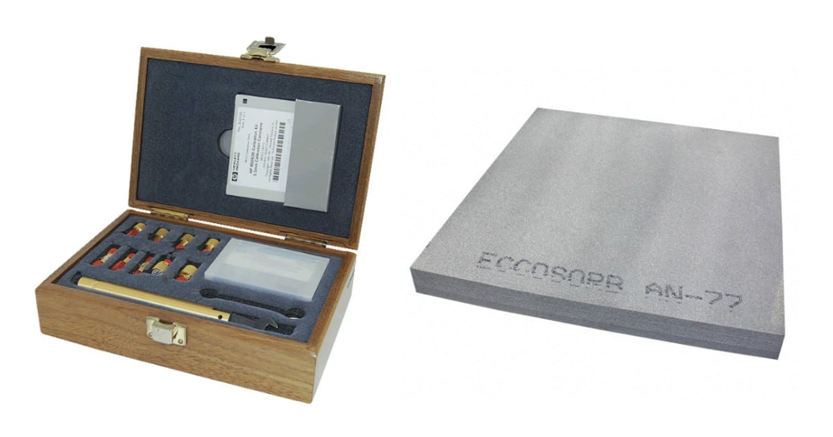
Let’s also assume the customer requires us to use RAM from Laird’s Eccosorb AN series and the maximum allowable RAM thickness is 10cm due to space constraints in the lab.
Selecting RAM
There’s an old adage in the test world: “test measurements are only as good as the test setup.” RF absorbers are no different.
Choosing the wrong absorber can introduce reflections that invalidate the measurement you are trying to make, defeating the entire purpose of this measurement process.
RAM effectiveness is highly dependent on frequency, thickness, material type, and test geometry.
The first step in selecting RAM is to determine the proper thickness needed to measure the antenna in the band of interest.
In our case, we need to calculate the maximum band quarter wavelength at fL = 1.4 GHz to roughly determine the minimum thickness necessary for the RAM.
Why a quarter wavelength? A wave travelling into the absorber and reflecting off the backing surface accumulates a round-trip path of half a wavelength — creating the destructive interference of the incident wave.
The actual electrical thickness is greater than the physical thickness, which means the free-space calculation is conservative for choosing the thickness of the RAM.
Choosing RAM based on higher frequencies within the band can lead to insufficient thickness at the low end.
This will increase reflections and degrade measurement accuracy. Hence why it’s important to calculate the lowest frequency’s quarter wavelength as opposed to frequencies above it.
Let’s calculate the quarter wavelength for the lowest frequency in the band of interest.
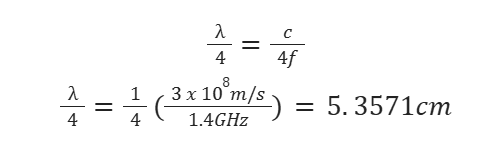
At minimum, the thickness of the RAM needs to be 5.3571cm to handle the 1.4 GHz – 3.4 GHz frequency band.
The second step in selecting RAM is to take the frequency band of interest and observe the reflectivity vs. frequency charts (in our case, on the Eccosorb AN datasheet).
Most RAM datasheets will show reflectivity vs. frequency (typically in dB). For S11-based validation, you typically want -20 dB reflectivity in the band of interest. Preferably -30dB for higher accuracy.
Once you hit -10 dB reflectivity in the band of interest, measurements start becoming unreliable due to reflections induced by the absorber itself.
Let’s take a look at the reflectivity vs. frequency plots from the Eccosorb AN series to determine the best reflectivity vs. frequency response for our application.
We also need to make sure the nominal thickness of the RAM matches our maximum quarter wavelength of 5.3571cm at 1.4GHz.
Enjoying this article?
Subscribe to Interference Technology for expert coverage of EMI, EMC, and signal integrity challenges—plus immediate access to new digital magazine issues.
Subscribe here →
Reflectivity vs. Frequency:

Reflectivity Range/Nominal Thicknesses/Nominal Weight Tables:
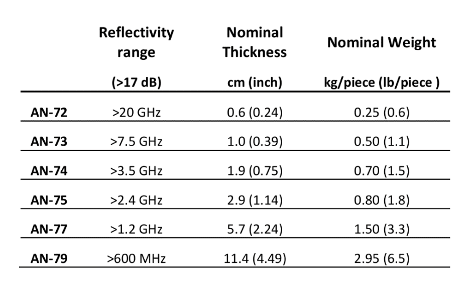
Based on the reflectivity vs. frequency chart plus the nominal thicknesses, AN-77 is the suitable option for this application based on the maximum quarter wavelength of the band of interest, reflectivity, and lab real estate.
Here’s the following checklist for this RAM:
- Is reflectivity across 1.4-3.4 GHz below -20 dB? Yes.
- Is the nominal thickness of the RAM above the maximum quarter wavelength of 5.3571cm at 1.4 GHz? Yes.
- Is the nominal thickness of the material below the 10cm constraint from the physical space in the lab? Yes.
Side note: if there were no physical thickness constraint in the lab, AN-79 would also be a suitable option.
Finally, you need to cut the RAM as this specific planar material comes in a sheet. Planar RF absorbers can be easily cut to size using a sharp utility knife or electric blade, depending on the thickness and material type.
It’s important to ensure clean, straight cuts and full coverage of the area beneath the antenna to avoid gaps or exposed edges that can introduce reflections.
The absorber should also extend well beyond the antenna’s physical footprint so that the radiated fields primarily interact with the absorber rather than edges or surrounding objects.
A good rule of thumb is that the absorber should extend at least half a wavelength or a full wavelength in all directions beyond the antenna. If the lab has space, go with a full wavelength to be safe.
For this application, the absorber should be extended roughly 21.5cm in length and width from the antenna, as the full wavelength at 1.4 GHz is 21.4286cm.

Configure Full Setup with RAM and VNA
As mentioned previously, the radiating side of the antenna needs to be placed face down on the RAM with the probe-side portion of the antenna facing upwards.
Next, configure the state file for LogMag S11 on the VNA to match the band of interest from 1.4 GHz – 3.4 GHz.
Choose a suitable step/resolution to capture the full response of the antenna; a good guideline for sufficient measurement resolution is 201 points between the upper and lower frequencies.
Typically, a customer will provide some sort of test specification on how to configure the state file.
Ensure the SMA cables and adapter connections to the VNA are rated for the higher end of the frequency band of interest and above.
If the lab’s budget allows, get cables and adapters that well exceed the higher end of the frequency band of interest to be safe.
Before taking any measurements, calibrate the VNA across the predetermined state file to de-embed the measurement plane to the end of the SMA coax cable.
We are interested in the characteristics of the antenna, not the antenna plus the cable.
This calibration can be executed by performing a one port S.O.L (short, open, load) with a mechanical calibration kit or an electronic calibration module (ECAL).
Ensure the mechanical calibration kit or ECAL module covers the entire frequency band of interest. Save the state file post calibration.
Post-calibration, check a few things on the VNA. With nothing connected to the coax cable, S11 should read flat at 0dB across the entire frequency band.
If there’s significant ripple, double check cable wear, cable specifications, adapter specifications, or just recalibrate. Mechanical calibrations on a VNA are a manual process, as opposed to ECAL.
I have personally mixed up many mechanical calibrations (connecting an open for a short measurement and vice versa), so sometimes recalibrating is all that’s needed.
Another post-calibration validity check would be to attach a known calibration standard to the SMA cable.
For example, if you attach a 50 ohm load standard directly to the SMA cable, S11 should read around -30 dB (sometimes -40 dB to -50 dB) for a high-end analyzer.

Post-calibration, connect the end of the SMA coax cable to the SMA connector site on the antenna.
If the connector requires it, always utilize a calibrated torque wrench to secure the cable directly to the device.
If there’s a little bit of freedom with the setup, I would still steer away from using SMA snap-on adapters — even if they are still accounted for in the calibration.
From my experience, SMA snap-on adapters can introduce variability in the measurements as the snap-on moves around due to the connector-to-adapter tolerance.
In general, you want to reduce any movement or instability in the cable or adapter to reduce measurement variation. Try to keep the setup as static and repeatable as possible.
Finally, execute a single sweep and extract the touchstone .s1p file for analysis and official record of measurement.
I encourage the reader to take S11 measurements with and without the RF absorber setup.
In practice, measurements without absorber often exhibit increased S11 ripple and distorted resonance due to external environment reflections from the antenna.
Troubleshooting
It’s also critical to distinguish what a bad S11 measurement can look like with a correct setup under the assumption that the device is designed and simulated correctly.
If S11 reads in the -2 dB to -5 dB ballpark range, follow this generalized checklist:
- Check the cables and adapters for wear and tear. Cables and adapters are consumables and will eventually degrade after excessive use. Check the cable and adapter datasheets for the allowed number of cycles. Swap out cables and adapters and recalibrate.
- If the analyzer has the feature, perform a time domain reflectometry (TDR) measurement to determine where the impedance mismatch is on the device. Refer to the equipment manual for how to perform the measurement and calculate distance utilizing time markers with proper amplitude selection.
- X-ray the failing site to check for solder voids, solder balls, cracks, or pin-to-ground solder shorts. Rework the connector or replace it entirely with sufficient solder connection. Remeasure the site and see if the response improves. Also, check for flattened pins causing a short between the pin and casing – another common connector issue caused by another process or the VNA probe itself.
- If possible, remove the connector site and utilize a pogo probe to measure the pad/site itself. If S11 shows the expected response, the issue is with the solder process or the connector itself.
If S11 has the expected designed/simulated response, but the trace has consistently stepped ripple, check the calibration validity with a 50 ohm calibration standard and when the last calibration was.
If S11 is only reading -15 dB to -20 dB across the whole band of interest and the calibration was last executed 24 hours ago, recalibrate.
The last resort is destructive failure analysis to pinpoint and fully understand the failure from a bareboard PCB standpoint.
This is a last resort and should only be performed after a thorough analysis from the RF Test Engineer.
RF Absorber and S11 Limitations
Just to reiterate, evaluating radiating PCBs using RF absorber and S11 measurements is only a halfway solution to capturing full antenna characteristics.
Even with decent reflectivity, the absorber still introduces some reflection into the antenna.
Also, S11 is a scalar reflection metric. It tells you nothing about the radiation pattern, directivity, gain, and polarization of the antenna itself — only if it is well-matched in the band of interest.
Think of RF absorber and S11 measurements as a power acceptance/environmental interaction measurement instead of a pure radiation measurement.
Conclusion
Using RF Absorber and S11 to evaluate these radiating structures is useful for getting a general understanding of how well-matched the structure is.
Many production environments utilize this setup. I myself used this setup when I was an RF Test Engineer. It’s reliable, quick to use, and easy to set up following the methods laid out in this article.
This setup does come with tradeoffs. If the goal is to capture full antenna characteristics, a full anechoic chamber isn’t just recommended, but necessary.
If the goal is to quickly confirm if the radiating PCB is fabricated correctly from customer requirements, using RF absorber and S11 measurements is a great solution for production environments.