
One challenge for EMC engineers is the impossibility of visualizing electromagnetic fields with our own eyes. Since we cannot directly observe them, we need tools to transform what we cannot see into what we can see.
There are a lot of EMC tools to measure and troubleshoot EMC problems, but their elevated price makes them accessible to only a select group of people. The combination of limited available time and the lack of affordable tools makes entering EMC difficult.
Near-field probes are fantastic for observing in real-time the effects of electromagnetic laws. There are two ways to get near-field probes: we can buy a new kit from the market, or we can build one by ourselves.
Designing and building near-field probes might seem unnecessary. Why build new ones when you can just buy a kit? Purchasing a kit provides speed, which is crucial during critical troubleshooting periods.
However, building a probe from scratch helps you understand the fundamentals of electromagnetism and master the intricate details of sources, transmission paths, and noise coupling.
This article covers the fundamentals of near-field probes, their types and properties, and will guide you on how to build your own printed circuit board (PCB) kit using KiCAD. You can find details of the designs in this public repository. [1]
UNDERSTANDING NEAR-FIELD PROBES
What Are Near-Field Probes?
Near-field probes are transducers that convert alternating magnetic fields (H) into currents and alternating electric fields (E) into voltages.
This selectivity makes them good tools for identifying sources of unwanted electromagnetic signals. The voltages they generate can be measured using a spectrum analyzer or a similar measurement device.
They are widely used to troubleshoot EMC issues in PCBs or electronic systems, as well as in integrated circuits (IC).
TYPES OF NEAR-FIELD PROBES
H-field Probes
H-field probes, or magnetic field probes, are designed to detect alternating currents.
They sense changes in the magnetic field, which are converted into alternating currents that can be measured. They are shielded against electric fields (or they should be), so they are specially designed to react to changes in magnetic fields. [Figure 1]

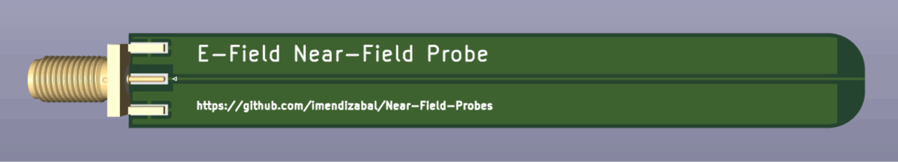
E-field Probes
E-field probes, or electric field probes, are designed to detect alternating voltages.
They work by sensing changes in the electric field, which are converted into alternating voltages that can be measured with a measurement device. [Figure 2]

KEY PARAMETERS
Before jumping into a CAD tool to design a new probe, you need to have a rough idea of the problem you are trying to solve. This makes it easier to define the design parameters.
It is important to know what matter the most, since there is a compromise between the different design parameters.
Frequency Range
What the probes measure depends a lot on the frequency. This is because the electromagnetic fields and their generated currents or voltages are highly dependent on the rate of change in the electric or magnetic field (i.e., the frequency), according to Maxwell’s laws:

A probe’s response varies significantly across different frequency ranges, affecting its effectiveness in detecting specific signals.
We need to know, even roughly, the frequency interval we are targeting. That will determine the probe size, materials, and shielding.
Sensitivity
Sensitivity is the minimum amount of signal that can be measured. The higher the sensitivity, the smaller the field that can be detected.
Different factors impact probe sensitivity: impedance mismatches, material losses, and frequency response. It is common to use probes of different sizes with different sensitivities.
Spatial Resolution
Spatial resolution is the smallest distance over which a probe can distinguish variations in electromagnetic fields. This factor is highly dependent on the type of electronic product being analyzed.
High-speed and densely packed communication boards need probes with extremely fine spatial resolution to accurately detect localized sources of interference.
On the other hand, in power electronics, with components such as large chokes and wide traces, a probe with lower spatial resolution is often sufficient to capture meaningful measurements.
Shielding
Shielding ensures that the probe measures only the intended signals and rejects others. Shielding is directly related to accuracy and reliability.
Without adequate shielding, signals from nearby components or external sources can couple into the probe and generate misleading measurements.
Enjoying this article?
Subscribe to Interference Technology for expert coverage of EMI, EMC, and signal integrity challenges—plus immediate access to new digital magazine issues.
Subscribe here →
WHY DESIGN YOUR OWN KIT?
Why design and build near-field probes instead of buying off-the-shelf options? There are good reasons to do it:
-
- Lower Costs: Commercial probes can cost hundreds or even thousands of dollars. By creating your own, you can significantly reduce expenses without sacrificing performance.
-
- Customization: Each PCB design has unique challenges. While it is common to buy a kit that covers 80% of the cases, a DIY kit allows you to experiment with sizes, shapes, and materials for specific tasks like diagnosing E-field or H-field interference in specific electronic systems.
-
- Deeper Understanding: Building probes from scratch provides hands-on learning about electromagnetic principles, like Maxwell’s equations. While watching videos is helpful, doing it by yourself will move you further.
A custom-built kit provides a flexible testing solution tailored to your design’s unique challenges, something mass-produced probes cannot match.
This project helps you master EMI detection and mitigation while fostering a mindset of innovation and precision — essential for today’s hardware designers.
DESIGNING YOUR PCB NEAR-FIELD PROBES KIT
Now it is time to build our own probes. There are different ways to do it, such as with a PCB or a coaxial cable. We will see how to design our own PCB kit and detail how to design a E-field probe.
Design Parameters to Consider
Once we know the important parameters of the performance of the probes (frequency response, sensitivity, resolution), we need to link these parameters with the PCB design parameters.
The key parameters are:
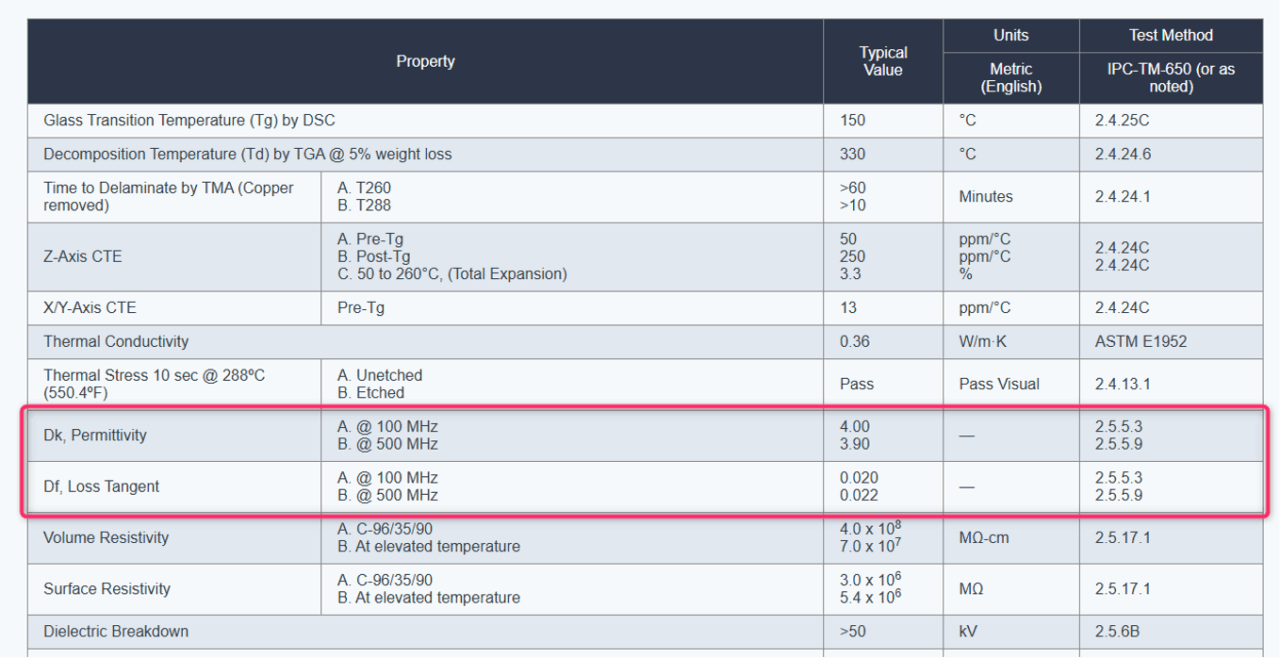
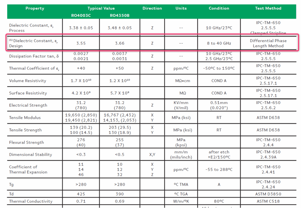
1. Dielectric Materials: Electromagnetic fields move within the material, not the copper. Dielectric material properties like dielectric permittivity (εr) will determine the frequency limitations of the probes.
2. PCB Stackup: The arrangement of signal and reference layers will impact the impedance of the traces. A proper arrangement will reduce unwanted noise pickup and increase the probe sensitivity.
3. Via Stitching: Using vias is a known technique to confine electromagnetic fields within a PCB. We will use the same principle to enhance the probe shielding, preventing signal leakage and interferences with other fields.
4. Ground Planes: Solid ground planes are key to provide a low-impedance return path to the high-frequency signals and keep a controlled impedance.
A careful selection of these parameters will provide optimal performance on the near field probes.
Selecting the PCB Materials
The material used for most of the PCBs is FR-4. It has low losses until reaching some GHz. For the most common measurements, FR-4 is enough.
However, if you plan to measure in the GHz band, it is recommended to use a material with a constant dielectric permittivity within the whole frequency range.
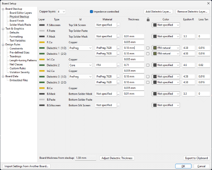
PCB Stackup
We need to find a trade-off between cost and performance. While a 2-layer board will be the cheapest, it reduces the possibility of adding solid ground planes or route traces internally.
The price reduction would not be as valuable as the loss of shielding, frequency range, or accuracy.
Today, the price for a 4-layer PCB is not much higher than a 2-layer PCB, and it will let us use solid ground planes. [Figure 5]
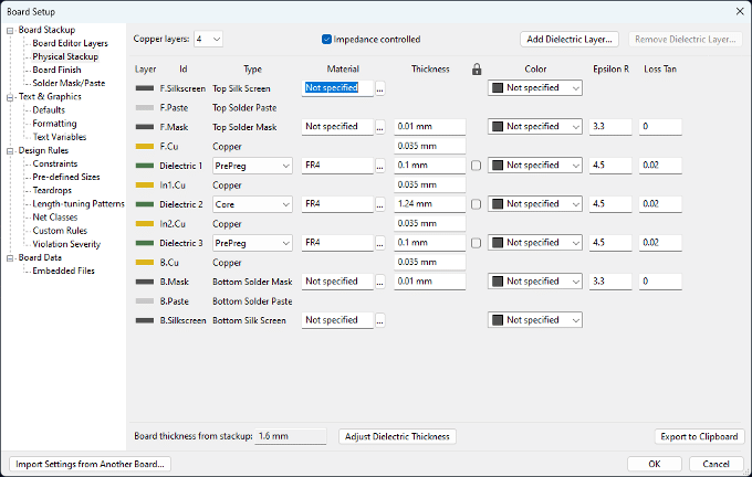

It is important to adjust the PCB stackup parameters according to your PCB manufacturer, so the manufactured product is as similar as possible to the designed one.
As an example, a regular 4-layer stack-up of the PCB manufacturer, highlighting the relevant parameters, is as follows; the resultant board setup in KiCAD will be Figure 6:
Routing
The routing of the trace signals and their reference planes play a vital role in the effectiveness of the probes.
In a 4-layer board, there should be one solid ground plane to route the signal with a controlled impedance. A second one can be added to improve the shielding of the traces.
The simplest option is to use the top layer to route the signal while keeping the rest for ground planes. The routing will be direct, without vias, reducing the capacitance and the parasitic inductances to their minimum.
Since the trace that will pick up the fields is exposed, the sensitivity will be high. The biggest disadvantage is the lack of shielding.
Via Stitching
Very often, we use vias to provide a low-impedance connection to planes, reducing any extra parasitic inductance.
Also, vias are useful to provide shielding: they protect the board signals against external noise and they help contain the fields within the board.
Then, in our probes, we will need vias for both purposes.
First, vias around the trace should be spaced close enough to shield against the highest frequency of concern. There are many rules of thumb defining the maximum distance of consecutive vias (λ/10, λ/20…).
The vias can be made very close as long as you do not violate hole-to-hole clearance limits imposed by manufacturing constraints.
While it is safe to apply them, do not forget:
- The value of the dielectric permeability when calculating the wavelength
- There is no additional price increase when adding vias
CONCLUSIONS AND NEXT STEPS
The article showed a step-by-step guide on how to design your own kit of PCB near-field probes. They are an easy and affordable method to start troubleshooting EMC problems and look for sources of electromagnetic emissions.
The design files are shared in a public repository, so you can manufacture and start measuring fast. The repository is a growing project, so it will be completed with more probes and information.
The next steps will be to design variants of the near-field probes so we can have probes of different sensitivities and space resolution.
REFERENCES
[1] Near Field Probes Github Repository. Available: https://github.com/imendizabal/Near-Field-Probes
[2] IS400 material datasheet. Available: https://www.isola-group.com/wp-content/uploads/data-sheets/is400-laminate-and-prepreg-isola-group.pdf?t=1196822952
[3] Rogers RO400. Available: https://www.rogerscorp.com/-/media/project/rogerscorp/documents/advanced-electronics-solu-tions/english/data-sheets/ro4000-laminates-ro4003c-and-ro4350b—data-sheet.pdf