
Many designers struggle with EMI and EMC challenges, and there are many myths surrounding EMI that do not help designers overcome EMC hurdles.
Some designers may lack experience, while others may know EMI/EMC rules but apply them incorrectly. There is also an issue of delegation, where EMI/EMC is sometimes seen as not being a designer’s problem.
No matter who is responsible for identifying and solving EMI problems, relying on old myths and design guidance is not the path forward.
To help you find real solutions to trouble-some EMI problems, we compiled a list of longstanding EMI myths in PCB design. With each of these myths, we’ve identified an appropriate design practice you can implement in your PCB to help suppress EMI.
EMI/EMC MYTHS WE LOVE TO HATE
Myth #1: Ground Planes Are for “Advanced” Designs
The most common EMI myth among new designers is not specifically about EMI, but rather about the use of ground planes in a PCB.
Some designers prefer to lay out and route a board on only two layers, and as a result they will not include a full internal ground plane. They might then include a grounded copper pour; this practice is discussed more below.
The reality is that many EMI problems can be solved sim-ply by using ground planes in a PCB. This also helps solve common problems in areas of signal integrity and power integrity.
Some important characteristics of ground planes in PCB design are outlined in the following table:
|
ROUTING |
|
|
SHIELDING |
|
|
RETURN PATH |
|
Myth #2: Splitting Planes Confines Noise
What’s more important than the presence of planes is how you use them, and unfortunately, there is one mixed-signal design practice that is responsible for many EMC failures.
Namely, the use of physically disconnected planes that confine analog and digital signals to different regions of the board.
There are a few reasons why this practice arises:
- There is a perception that analog and digital power circuits cannot share a ground net.
- Pin naming on ADCs and DACs creates the impression that grounds should be separated.
- The designer misunderstands how return currents flow in relation to frequency.
- The designer misunderstands ground loops and believes that split planes will eliminate them.
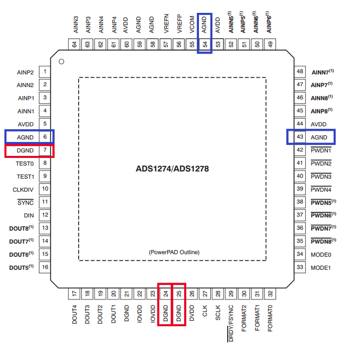
ADCs are one component where the pin naming can create a perception that planes need to be physically split into analog and digital sections. Very clear guidance in datasheets often reveals that this is not the case. Consider, for example, the ADC pinout shown below.
This one practice has caused more EMC failures than any of the other myths we discuss in this article. It also leads to bad routing practices, where signals are routed across splits in a ground or power plane, resulting in radiated EMI.
Split planes can be used in PCBs, but they place many mixed-signal designs at risk of a radiated emissions failure.
The safest approach to the use of split planes is that they should be limited to cases that require galvanic isolation or precision measurement of low-amplitude signals.
Enjoying this article?
Subscribe to Interference Technology for expert coverage of EMI, EMC, and signal integrity challenges—plus immediate access to new digital magazine issues.
Subscribe here →
Myth #3: You’ll Pass EMC with Copper Pour and Stitching Vias
Copper pour with stitching vias is another technique often used as a cure-all for noise problems.
Copper pour and stitching vias are useful in low-density, two-layer PCBs because they provide effective ground connections, and they can help prevent radiated EMI in these designs. They can also shield specific interconnects from receiving noise and thereby reduce EMI susceptibility.
In designs with four or more layers and uniform internal ground planes, stitching vias and copper pour are not guaranteed to solve all radiated EMI problems, though they might conceal a radiated EMI problem by providing shielding.
Instead of relying on copper pour and stitching vias with the intention of suppressing noise, focus on stack-up and routing, and you may find that a copper pour with stitching vias is not needed.
Myth #4: Right-Angle Traces Create EMI
This particular myth is very persistent, despite the preponderance of evidence that 90-degree traces are not generators of strong EMI.
It is true that each bend creates excess fringing capacitance of <1 pF at the bend, but this amounts to an impedance deviation of approximately 1% in the bend region for a 50 Ω line.
The idea that a right-angle trace will create excess EMI is silly and should be ignored. The potential reflection problems created by 90-degree angles do not become noticeable until a design is operating in the very high GHz range, such as at mmWave sensor frequencies (60 GHz) or car radar frequencies (77 GHz).
This is why many RF designs use curved traces. Every source of impedance deviation and excess loss is being avoided in these designs, but this is done to enhance signal integrity, not to prevent EMI.
RULES-BASED APPROACHES FOR EMI CHECKING
Simulation software vendors have developed many simulation tools for predicting EMI problems; these range from equivalent SPICE models to full-wave electromagnetic field solvers.
These software tools are very useful, but EMI problems can often be caught more efficiently with a rules-based EMI checking approach.
This allows designers to catch errors early and address them quickly, before placing a design into a full-wave solver.