Introduction
To start at the very beginning, what is an electrical filter? An electrical filter can be passive, active, analog, or digital. It is a device usually composed of discrete components which can be placed between circuits, networks, or equipment/systems to either emphasize, de-emphasize or control the frequency components of a desired or undesired signal. The term “signal” can be a communication or power type signal. Filters accept an electrical signal at its input and deliver a different or modified signal at its output depending upon the filters internal configuration. The general term filter, of course, can also be used for a device on control and signal type lines. However, for this article, we will focus on the AC/Mains EMI (ElectroMagnetic Interference) power type filter.
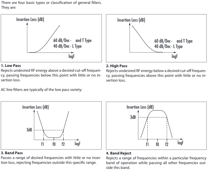
Filter Classifications:
Why Do We Need EMI Filters?
One reason is that regulatory agency requirements dictate that conducted and radiated emissions be constrained below specified limits, but the unit must also pass immunity/transient requirements. Designers often forget that an EMI filter can assist in meeting immunity and fast transients requirements and radiated emissions as well. Even for military/aerospace equipment, they must be protected from failure due to EMI noise and security requirements may call for filters to protect classified data. Contractual requirements imply or specify filters.
Essentially, an AC power or mains EMI filter is a low pass filter that blocks the flow of “noise” while passing the desired input which can be DC or 50/60/400 Hertz power frequency. An ideal EMI filter will reduce the amplitude of all frequency signals greater than the filter cut-off frequency. The cut-off frequency is the frequency between the signal’s passband and the reject bands at 3 dB attenuation below the acceptance line. The measure of a filter’s ability to reduce a given signal level is insertion loss or attenuation. A power line or mains EMI filter is placed at the power entry point of the equipment that it is being installed into to prevent noise from exiting or entering the equipment.
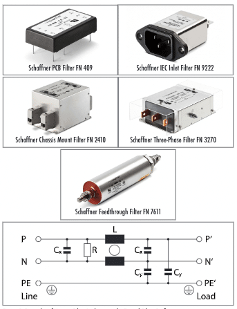
Filter Configurations
Essentially, an EMI filter is made up of two basic types of components–capacitors and inductors. The simplest type is called a first-order filter consisting of just a single reactive component. Capacitors shunt noise current away from a load while inductors block or reduce the noise. Generally, these single component filters are not very useful as their attenuation only increases at a rate of 6 dB/octave or 20 dB/decade.

To achieve greater attenuation, a second or higher-order filter as shown in Figure 3 consisting of two reactive components or more is required. The value of the inductive or capacitive components is determined by the impedance of the source, load and the highest frequency to be passed (i.e. cutoff frequency). This two-element filter is sometimes referred to as an “L” filter. Filter resonances and ringing must be considered, and involves a design characteristic called damping factor which describes gain and the time response of the filter.

A third-order filter, of course, consists of three or more re-active elements as shown in Figure 4. These types of filters are sometimes referred to as “pi (π)” or “T” filters. The disadvantage of a larger filter is that physical size increases. The third-order filter is among the most popular topologies of filters used.

How to Determine Which Configuration to Use
Impedance Mismatch
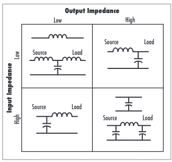
Two different circuit configurations exist for the higher order filters in Figures 3 and 4. One aspect of filter design is impedance mismatch. So, which one should the designer use. If the designer has access to computer simulation software, then it can be used to determine the best configuration. However, if a simulation program is not available, then there is a simple “rule of thumb” that can be used to assist the designer. The first filter element nearest the source, or load end, should be selected to provide the highest possible mismatch at EMI frequencies. Typically, this means that if the source or load impedance is low (<100 Ohms), then the first filter element should be an inductive component. Conversely, if the source or load impedance is high (>100 Ohms), the first filter element should be capacitive. This provides the designer an extremely efficient design with the least number of stages or components. Refer to Figure 5 as a quick, handy guide.
Common-Mode Currents versus Differential- Mode Currents
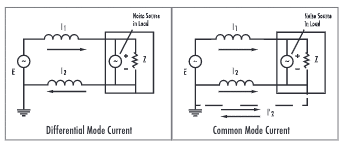
Filters are not only for conducted emissions, but also help in meeting radiated emissions levels by controlling what prop-agate from the mains power cable and also helps in immunity issues like induced RF (Radio Frequency) signals and transients like electrical fast transients (EFT). In all circuits both common-mode (CM) and differential-mode (DM) currents are present. There is a significant difference between the two. Given a pair of transmission lines and a return path, one or the other mode will exist, usually both. Differential-mode signals carry data or a signal of interest (information). Common-mode is an undesired side effect from differential-mode transmission and is most troublesome for EMC.
When using simulation software to predict emissions, differential-mode analysis is usually the form of analysis used. It is impossible to predict radiated emissions based solely on differential-mode (transmission-line) currents. Common-mode currents are the primary source of EMI. If only calculating differential-mode currents, one can severely under-predict anticipated radiated emissions since numerous factors and parasitic parameters are involved in the creation of common-mode currents from differential-mode voltage sources. These parameters usually cannot be easily anticipated and are present in the formation of power surges in the power and return planes during edge switching times.
Differential-mode current is the component of RF energy present on both the signal and return paths that is equal and opposite of each other. If a 180° phase shift is established precisely, RF differential-mode currents will be canceled. Common-mode effects may however, be developed because of ground bounce and power plane fluctuation caused by components drawing current from a power distribution network.
Using differential-mode signaling, a device sends out current that is received by a load. An equal value of return cur-rent must be present. These two currents, traveling in opposite directions, represent standard differential-mode operation. Differential-mode filtering involves placing capacitors between lines and/or an inductor in series with either the high or low side of the line. Reference Figure 7.

Common-mode current is the component of RF energy that is present on both signal and return paths, often in common phase to each other. The measured RF field due to common-mode currents will be the sum of the currents that exist in both the signal and return trace. This summation could be substantial. Common-mode currents are generated by any imbalance in the circuit. Radiated emissions are the result of such imbalance.
Common-mode filtering involves capacitors to ground and/or a common mode inductor in series with both side of the line or lines. A common-mode inductor does not affect differential-mode currents except for whatever imperfect coupling exists (i.e., leakage inductance). It is best to split the inductor evenly on both sides of the transmission line to maintain balance in the circuit. This is important for both common-mode and common-mode rejection ratio of the circuit. Mutual inductance will maximize the impedance to common-mode noise. Reference Figure 8.
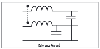
Because these are two different noise current modes of propagation, it is important to determine which type of noise current exists so that proper filtering can be implemented for maximum efficiency and cost. This is important for both common-mode and common-mode rejection ratio of the circuit. One can see that most typical filter configurations contains both common mode and differential mode filtering as shown in Figure 6.
Layout Hints
We will discuss the advantages and disadvantages of open printed circuit board (PCB) constructed filters versus filters in a metal can shield. There are two types of noise coupling (radiated and conducted). Radiated and conducted noise has a tendency for mutual transformation through a wire or trace by a process termed crosstalk. Crosstalk is observed where there are many wires or traces located in close proximity. Therefore, even if conducted noise is only a problem at one location, you cannot completely ignore the possibility of radiated coupling to another location. So, if a filter circuit is incorporated on a printed circuit board, then proper de-sign and layout techniques must be done such as avoiding routing of traces parallel to each other, providing sufficient separation between traces to minimize inductive coupling or routing adjacent layers (microstrip or stripline) orthogonally to each other to prevent noise coupling between traces. See Figure 9. However, with the use of a metal shield, crosstalk/radiated noise coupling crosstalk is controlled.
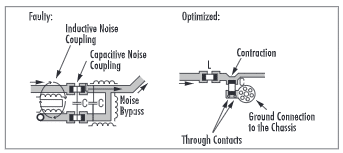
Other things to consider are the high frequency parasitic and resonance effects. Real inductors and capacitors fall short in performance when compared to theoretical models. Some of this is due to the actual inductor and capacitor elements themselves (e.g. lead inductance, winding capacitance, resistance effects, etc.) while others are caused by the circuit board layout, packaging or wiring. Changing to a different EMI filter can affect the radiated emission characteristic be-cause of these parasitic and resonance effects. So, when you change from a filter that passes testing, one must re-test not only for conducted emissions, but also re-test for radiated emission as the high frequency effects may not be the same between the two filters especially since most commercial filters are never tested beyond 30 MHz.
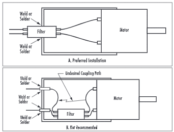
The filter should be placed directly at the exit point of the wire from the product. Good effective separation is essential. The separation prevents coupling of noise back into the input wires circumventing and nullifying the effects of the filter. This would be an excellent choice for an AC inlet mounted EMI filter or “power entry module (filter)”.
To go along with the above item, avoid improper lead rout-ing. Do not bundle or physically cross filter input and output wires. Again, with the leads physically crossing each other, it nullifies the effectiveness of the filter due crosstalk between wires as was discussed earlier.
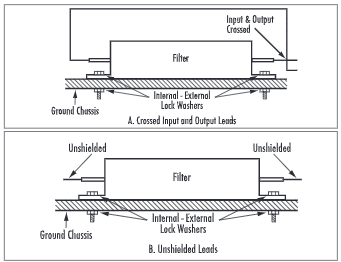
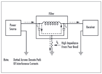
Provide a low impedance ground for the filter. It is imperative that the EMI filter mounting surface be clean and unpaint-ed (e.g. conductive surface). Good filter grounding is an im-portant factor for common mode filtering performance of the filter. A poor filter bond limits the filtering to chassis by adding series impedance, thus changing resonance effects and filtering capability of the common mode capacitors. See Figure 12.
Final Thought
Commercial filters are available for various applications with different insertion loss. There are other features to consider like Earth leakage, ambient temperature and over load characteristics. Before going to the test lab, procure different filter configurations from a commercial filter company to have on hand during testing. If the original one doesn’t pass, then change over to an alternate one. Having them on hand will shorten the development time and save on test lab cost due to multiple revisits.
References
1. A Handbook on Electrical Filters, Donald R.J. White, Germantown, MD, Third Printing 1970.
2. The EMC Desk Reference Encyclopedia, Don White, emf-emi control inc., Gainesville, VA, 1997.
3. Testing for EMC Compliance, Mark I. Montrose and Edward M. Nakauchi, John Wiley & Sons, Inc. 2004.
4. Interference Reduction Guide For Design Engineers – Volume II, National Technical Information Services, US Department of Commerce, Springfield, VA, August 1964.
5. Trilogy of Magnetics, Würth Electronik eiSos GmbH & Co KG, Edition 4, 2010 (ISBN 978-89929-157-5).


