
Verifying your trace S-parameters is more than just good practice—it’s essential for confident measurement, simulation, and design space exploration in modern EDA tools. Especially in high-speed digital systems where traces are long, applying a few key principles can provide valuable insights into your data and give you a head start in your design exploration.
TRUST BUT VERIFY YOUR TRACE S-PARAMETERS
As Dr. Eric Bogatin, the signal integrity evangelist, teaches in his Rule #9: “Never perform a measurement or simulation without anticipating what you expect to see” [1]. In this article, we will discuss what to expect from the S-parameters of a single-ended trace.
An S-parameter analysis is shown in Figure 1. A sine wave at a given frequency, f0, is launched at Port 1. The S11 represents the reflection coefficient and the return loss at Port 1. S21 represents the transmission coefficient and the insertion loss to Port 2.

Given a single-ended 6-inch trace, we will discuss four essential things to expect and check with your S-parameter data.
CHECK THE LOW-FREQUENCY BEHAVIOR (S11 AND S21 )
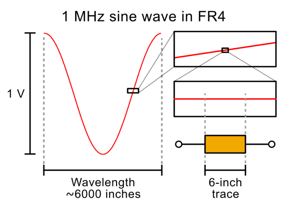
At the low end of the frequency, a few megahertz, a typical trace (a few inches) is very short compared to the wavelength of the stimulus signal.
For example, a 1 MHz sine wave in FR4 material has a wavelength of approximately 6000 inches.
A typical 6-inch trace is only 0.1% of the wavelength. Because the physical length of the trace is only 0.1% of the wavelength at 1 MHz, the signal experiences minimal phase change after traversing the trace, see Figure 2.
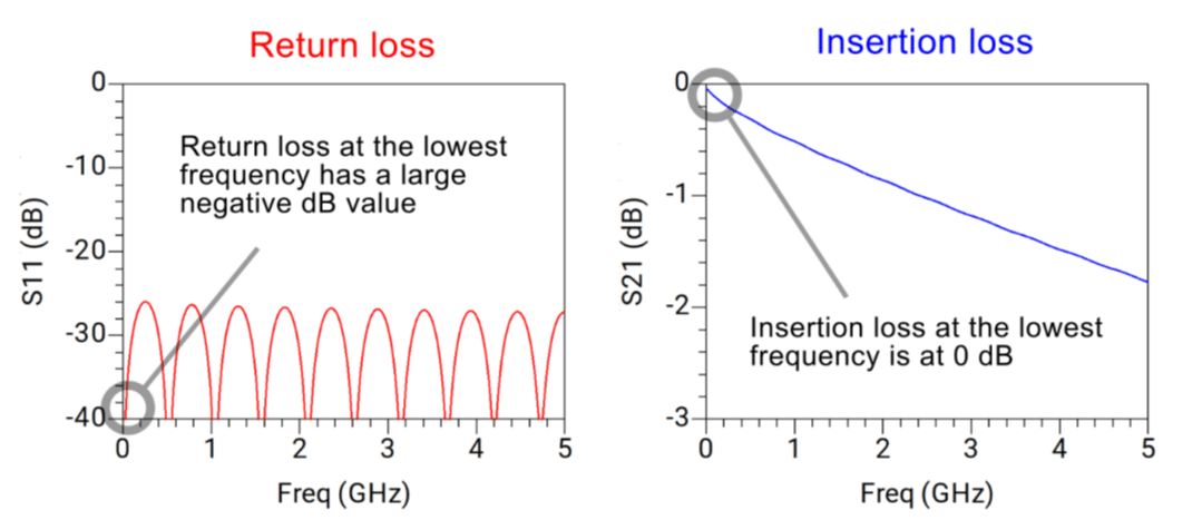
As a result, the trace would look transparent to the signal. At the lowest frequency, this means no signal is being reflected. The return loss, expressed in S11 in dB scale, has a large negative dB value at the lowest frequency.
Since no low-frequency signal is reflected, all must be transmitted. As a result, the insertion loss, expressed in S21 in dB scale, approaches 0 dB at the lowest frequency, as shown in Figure 3.
Enjoying this article?
Subscribe to Interference Technology for expert coverage of EMI, EMC, and signal integrity challenges—plus immediate access to new digital magazine issues.
Subscribe here →
SPOT THE FIRST S11 RESONANCE PEAK
Let’s assume this 6-inch trace has a characteristic trace impedance of 50 Ohms. Since all printed circuit board traces have loss, our assumed 50-ohm trace impedance will have an imaginary part. The trace impedance is a complex number.
In a typical S-parameter analysis, the reference impedance of the ports is 50 Ohms, a purely real number. This mismatch between the purely real port impedance and complex trace impedance creates reflections.
Constructive interference of reflections at Port 1 results in a peak in S11. When the reflections add destructively, we observe a dip in S11 , as shown in Figure 4.
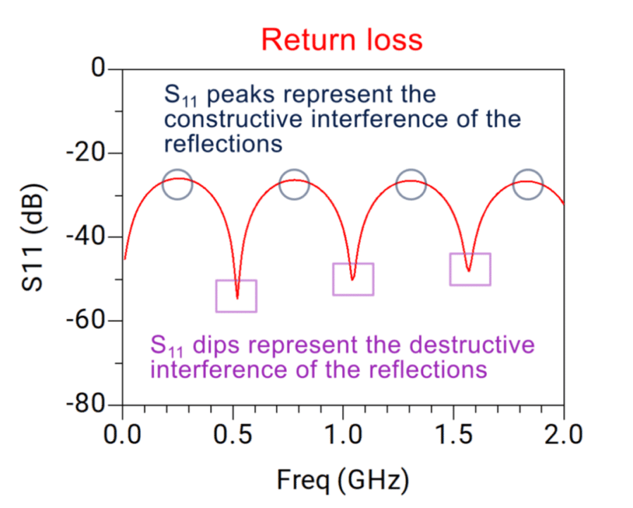
The first peak of S11 is the frequency where the physical length of the transmission line corresponds to a quarter of a wavelength. At this frequency, the reflection at port 1 adds constructively with the reflection from port 2, creating a peak in return loss.
The equation below helps you estimate the frequency at which you should expect the peak of S11.
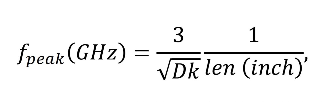
Assuming your substrate is FR4 and has the dielectric constant (Dk) of 4, and you have a strip line trace that is about 6 inches, you should expect the first return loss (S11 in dB) peak around 250 MHz, see Figure 5.
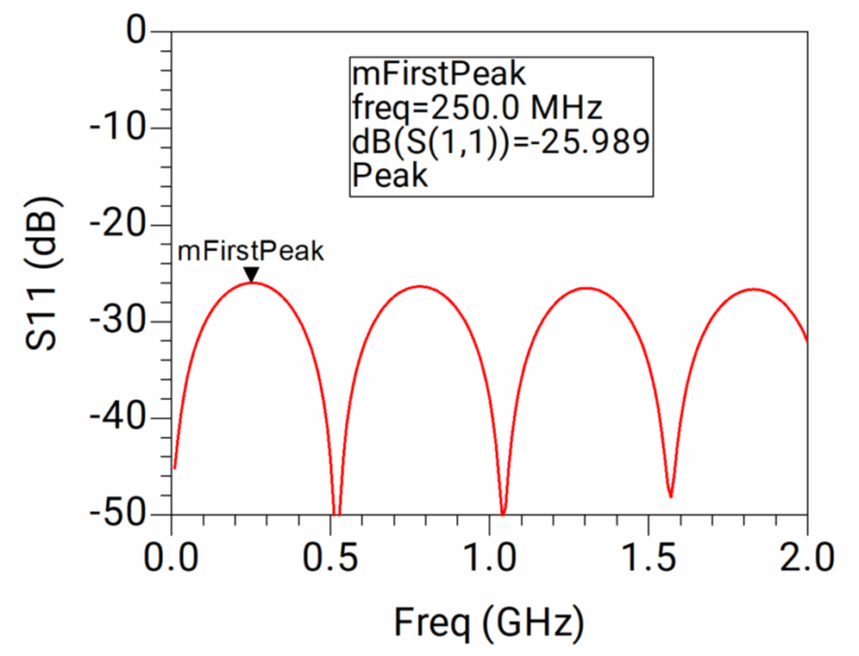
Typically, a microstrip line in an FR4 substrate has an effective Dk that will be lower than 4, which will increase the resonance frequency.
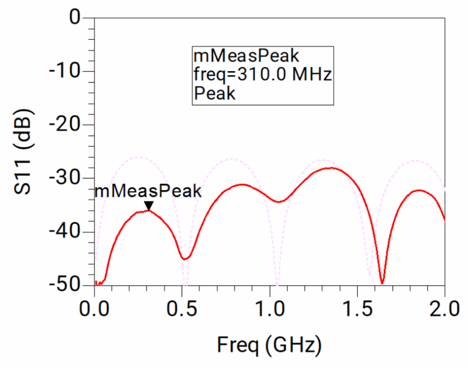
Figure 6 shows a measured 6-inch microstrip line. As expected, the first peak (310 MHz) is at a higher frequency than the simulated (250 MHz).
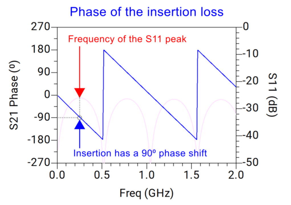
USE S21 PHASE AS A SANITY CHECK
Because the S11 peak is the result of the quarter-wavelength constructive interference, the phase of S21 should tell us a consistent story. That is, at the frequency where the S11 has a peak, the phase of S21 should be 90 degrees, indicating the quarter-wave nature of the interference.
As demonstrated in Figure 7 below, as we plot the S11 on the right y-axis and overlay the phase of S21 on the left y-axis, we notice the peaks of the S11 align with the 90-degree phase shift in the phase of S21 .
EXPECT RAMP-UP IN REAL MEASUREMENTS
So far, the S11 plot example appears clean and flat over all frequencies because the trace was created and solved using Controlled Impedance Line Designer (CILD) in Keysight Advanced Design System (ADS). The solver handles arbitrary dielectric layers and arbitrary metal thickness [2].
If the S-parameter of the trace is measured, one should expect the ripples to increase (ramp up) as the frequency increases, as shown in Figure 8 below.
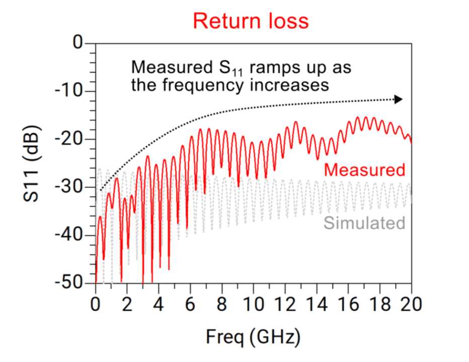
The small impedance discontinuities in the connectors or fixtures cause this behavior to happen. One should always expect a level of S11 ramp-up in S-parameter measurements. In practice, ripple ramp-up with frequency is a tell-tale sign of real-world discontinuities, such as fixtures or connectors.
SUMMARY: THINK LIKE AN SI DETECTIVE
S-parameter data can tell you more than what it shows. Like a good detective, you can question the evidence. These checks provided in the article help you:
- Validate measurement consistency and setup at low frequencies.
- Estimate trace length and match it to your expected behavior.
- Confirm quarter-wave effects using S21 phase as a sanity check.
- Spot a real measurement by watching for S11 ramp-up.
With these checks, you can extract not just confidence, but insight, from your S-parameters, setting yourself up for smarter simulation, cleaner correlation, and better signal integrity overall.
REFERENCES
- E. Bogatin, “Bogatin’s 20 Rules for Engineers,” Signal Integrity Journal, Feb. 3, 2020. [Online]. Available: https://www.signalintegrityjournal.com/blogs/4-eric-bogatin-signal-integrity-journal-technical-editor/post/1539-bogatins20-rules-for-engineers
- Keysight Technologies, Multilayer Interconnects – Advanced Design System 2025 Update 2 Documentation. [Online]. Available: https://docs.keysight.com/ads2025update2/component-libraries/components-analog-rf/distributed-components/multilayer-interconnects