As the semiconductor industry embraces the chiplet design approach, electrical engineers are witnessing a significant shift in how performance, cost efficiency, and scalability are achieved.
While this modular design philosophy offers advantages, it also introduces challenges to signal integrity (SI). For EMI/EMC engineers, the awareness of these signal integrity challenges is valuable because they intersect with broader system reliability concerns.
This knowledge will help you better anticipate and mitigate potential issues in chiplet-based designs. This article provides an overview of the chiplet system and covers:
- The rise of the chiplet design philosophy
- Signal integrity (SI) complexities in chiplet designs
- SI specifications for the electrical layers from the Universal Chiplet Interconnect Express (UCIe) standard
RISE OF CHIPLET DESIGNS
The shift towards chiplet design is a practical response to the need for cost-effective, low-risk semiconductor manufacturing processes [1].
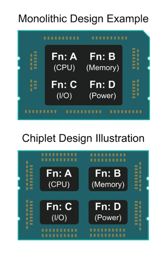
In traditional chip designs, better performance often means making the chip larger. However, with chiplet designs, shown in Figure 1, different functions are separated into smaller, individual chips.
This approach enhances cost efficiency, yield, and scalability. The term ‘chiplet’ denotes the compact size of each die/chip.
Enjoying this article?
Subscribe to Interference Technology for expert coverage of EMI, EMC, and signal integrity challenges—plus immediate access to new digital magazine issues.
Subscribe here →
COST AND YIELD
In practice, manufacturing the entirety of a larger chip design with the most advanced technology (advanced node) can cost almost twice as much as the chiplet approach [2]. Also, not all functions within a large design necessitate fabrication with the most advanced technology.
Larger chips in traditional designs are needed to boost computing power. This increase in size introduces two problems:
- The large reticle size can reach the fabrication limit
- The yield of the large reticle size can be too low to be profitable
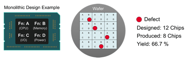
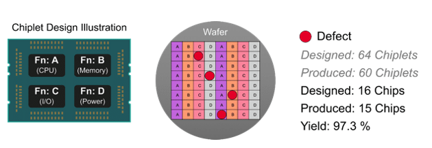
Figure 2 and Figure 3 compare the two design approaches using wafers of the same size and four similar defects.
Consider the example where a large monolithic chip requires four functional blocks — A, B, C, and D — to work. As illustrated in Figure 2, defects in functions A, B, C, or D on the same die render the entire die unusable. The yield for a monolithic approach is 66.7%.
On the other hand, because the chiplet design splits the chip functions into four smaller dies, if one defect is found on A, only the die with the particular function A is impacted, not the entire chip (A, B, C, and D).
In this case, the yield can be as high as 97.3% with the same four defects, as shown in Figure 3.
SIGNAL INTEGRITY CHALLENGES IN CHIPLET DESIGNS
Having discussed the cost and yield benefits, we now focus on the signal integrity challenges in chiplet designs.
Although the chiplet’s modular approach increases yield, the functional blocks are now on different dies. This introduces:
- Increased design complexity
- Challenges in chiplet die-to-die (D2D) communication
As a result, robust signal integrity analysis of the D2D communication is crucial in establishing the reliability and interoperability of chiplet-based designs.
Key components of D2D signal integrity (SI) include the following:
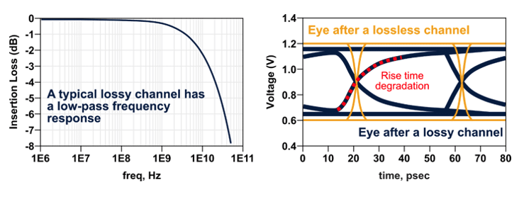
Loss
The frequency-dependent loss from D2D interconnects attenuates high-frequency components more than lower-frequency ones.
As shown in Figure 4, this low-pass behavior of the interconnect alters the frequency spectrum of the input data, causing rise time degradation.
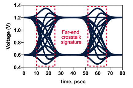
Crosstalk
As the interconnect density increases and signal traces are closer to each other, crosstalk becomes a primary signal integrity concern. Because of the interconnect’s physical proximity, the energy in adjacent interconnects can couple into the line of interest.
As shown in Figure 5, the crosstalk noise appears in the received eye as peaks in the transition region.
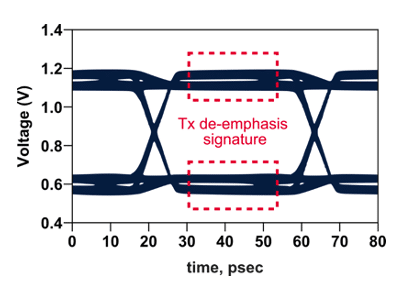
Transmitter and Receiver Configuration
As the optimization of the interconnect design reaches the final stages, one looks to the transmitter (Tx) and receiver (Rx) to further improve the signal integrity.
Termination strategies and equalization techniques can be applied to the transmitter and receivers. Figure 6 shows an example of a Tx eye diagram after applying de-emphasis.
SI GUIDANCE IN THE UCIe STANDARD
Recognizing the upcoming SI challenges in chiplet D2D interconnect designs, researchers and engineers have created standards to guide the industry. One such standard is the Universal Chiplet Interconnect Express (UCIe).
The UCIe standard not only provides physical dimensions for chiplet designs, but also offers electrical layer specifications on the SI of the interconnects. Below are three examples.
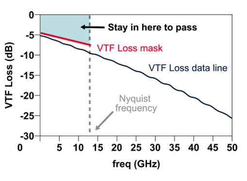
VTF Loss
The UCIe standard introduces a unique measurement called VTF, or voltage transfer function. As shown in Figure 7, the VTF loss metric is a mask that helps determine whether the current interconnect is too lossy.
To pass, the VTF loss line of your data line needs to be above the UCIe VTF loss mask.
The main difference between VTF loss and S-parameter insertion loss is that the former includes input and output resistance and capacitance in calculating VTF loss [3].
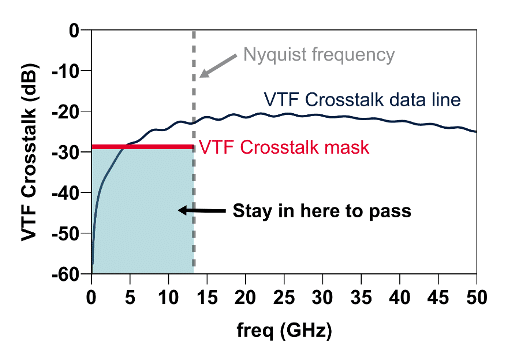
VTF Crosstalk
Similarly, the UCIe standard provides a mask for VTF crosstalk. VTF crosstalk is defined as the power sum of the ratios of the aggressor receiver voltage to the source voltage [3]. Figure 8 below is a data line that fails the VTF crosstalk metric.
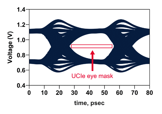
Eye Mask and Equalization
Figure 9 shows the UCIe standard specified eye masks for 24 GT/s (Giga-Transfer per second). The eye height is 40 mV and the eye width is 65% of the unit interval.
As the data rate reaches 24 GT/s or 32 GT/s, the UCIe standard requires the implementation of Tx equalization. Equalization (EQ) on the transmitter (Tx) is recommended for 16 GT/s. On the receiver (Rx) side, the standard states that equalization may be implemented at 24 GT/s and 32 GT/s [3].
CONCLUSION
While chiplets offer enhanced cost efficiency and scalability, they also introduce new complexities in die-to-die communication that can impact system performance.
As chiplet designs become increasingly prevalent in the semiconductor industry, understanding their benefits and challenges is valuable for EMI/EMC engineers.
By understanding chiplet designs and the Universal Chiplet Interconnect Express standard, engineers are better equipped to anticipate and address potential issues.
This knowledge is essential for optimizing design strategies, ensuring robust signal integrity, and achieving overall system reliability.
REFERENCES
[1] “Chiplets Are Revolutionizing Semiconductor Manufacturing with More Flexibility and Lower Costs,” [Online]. Available: https://sourceability.com/post/chiplets-are-revolutionizing-semiconductor-manufacturing-with-more-flexibility-and-lower-costs
[2] G. Loh, “An Overview of Chiplet Technology for the AMD EPYC™ and Ryzen™ Processor Families,” [Online Video], Available: https://youtu.be/wqRAG_5KzBE
[3] “Universal Chiplet Interconnect Express (UCIe) Specification,” July 10, 2023, Revision 1.1, Version 1.0.