ABSTRACT
Philosophies for the best method of HEMP protection have been around for a long time. MIL-STD-188-125 -1 and -2 are more recent specifications for defining requirements for HEMP protection. They specify PCI (pulse current injection) testing techniques to demonstrate the integrity of the protection system, but require specialist test equipment capable of injecting high voltage high current pulses. The residual current let-through of the protection system plus other parameters are monitored as a measure of the effectiveness and compliance of the protection system.
Because the demand for HEMP protection systems is specialized and not high volume, the practical method of meeting the MIL-STD-188-125-1 and -2 specifications has normally been based on adapting certain types of standard catalog EMI facility filters. However, most catalog EMI filters are designed for CW insertion loss performance, so are usually not ideal for pulse applications.
The approach described here is to design filters to meet a pulse attenuation performance rather than to meet an insertion loss specification. This enables a filter circuit and components to be used which are optimized for pulse applications to achieve a more efficient design with a good pulse performance.
This article describes the design process and validation of the design by testing using the MIL-STD-188-125 specified pulses.
INTRODUCTION
MIL-STD-188-125-1 and -2 specifications [1] & [2] cover HEMP protection requirements for fixed and transportable ground based installations respectively. They define three PCI pulse types for testing the integrity of the protection system, E1 (short pulse) 20/500ns 2.5kA peak, E2 (intermediate pulse) 1.5/4000µs 250A peak, and E3 (long pulse) 0.2/20s 1000A peak. The filter design discussed in this article addresses protection against the E1 and E2 pulses. Different techniques are needed to address the E3 pulse.
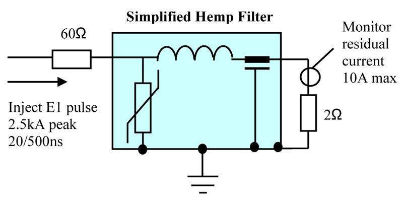
The procedure for checking compliance of a HEMP filter with the specification for the E1 pulse is to inject the pulse into the front end of the filter and monitor the residual current flowing through a 2 ohm resistive load connected between the output terminal and earth – see figure 1. For higher current filters the resistive load is replaced by one of value given by V/I where V and I are the voltage and current ratings of the filter. The simplified circuit shown is indicative only to show the key lumped elements. For the E1 pulse, the generator source resistance is specified as 60 ohms as shown in figure 1, so the peak applied voltage supplied by the generator needs to be 150kV. The maximum acceptable residual current through the 2 ohm load is 10A peak, and there are also limitations on residual pulse rise-time and energy.
For the E2 test, pulses are injected in a similar manner but there is no requirement to monitor the residual pulse. However, the filter must survive the pulse without damage.
To strictly comply with the requirements of the MIL-STD, every filter needs pulse testing both before and after installation.
NORMAL APPROACH TO HEMP PROTECTION
It is usually considered that there is insufficient demand for EMP protection systems to justify dedicated designs, so it is normal to select a standard catalog EMI filter and adapt it as necessary to meet the requirement. It is generally recognized that it is best to use an inductive input filter where possible and fit high energy transient suppressors at the front end to provide the pulse protection. When tested, the pulse attenuation performance offered may not be sufficient to meet the MIL-STD requirement, so remedial measures in the form of additional filter and suppression components may be needed to ensure compliance. Although with this approach there is little initial design cost, there may be major hidden costs in terms of the remedial action required to achieve compliance.
DEDICATED DESIGN APPROACH
Because most catalog EMI filters are designed for CW insertion loss performance rather than pulse handling, it was decided to design a range of filters from first principles to suit the pulse requirement of MIL-STD-188-125, i.e. to attenuate the magnitude of a 2500A 20/500ns E1 pulse to less than 10A, and to tolerate the E2 pulse. The transient suppressor, and filter capacitive and inductive components were treated as an integrated solution. Circuits were built and tested and pulse currents and voltages were monitored at each stage in the circuit to analyze the effect and contribution of each component and also the interaction between components.
DESIGN PHILOSOPHY
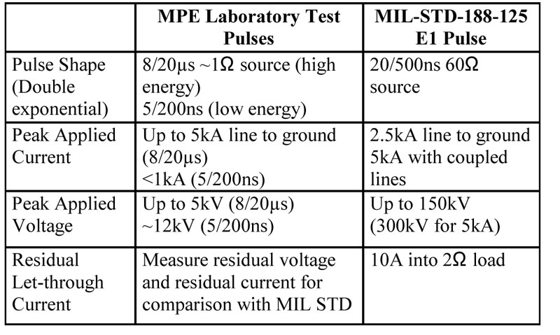
It was not practical to carry out development testing using the defined MIL-STD pulse waveforms because of their specialist nature, so it was necessary to use commercially available test equipment. This comprised an 8/20µs pulse tester for bulk current handling tests with a pulse current of up to 5kA, and a 5/200ns pulse tester for rise-time checks. The energy content of the 8/20µs pulse is higher than the MIL-STD E1 pulse but its rise-time is much slower. The 5/200ns pulse was used to demonstrate the speed of response of the system although its energy was very low, so most testing was concentrated on the 8/20µs pulse with a view to meeting the E1 residual current limit of 10A.
A comparison of MPE laboratory testing capability compared to the MIL-STD pulse requirement is given in table 1.
To meet the requirements of the E1 and E2 pulses, many types of transient suppression device were evaluated including spark gaps, metal oxide varistors (MOV’s), and silicon avalanche diodes. The varistor was finally chosen for this filter design because of its good combination of reaction time, when mounted effectively, and energy handling characteristics, making it suitable for both the E1 and E2 pulse requirements.
DEVELOPMENT TESTING
Circuits were built and tested based on the circuit shown in figure 2, as it was initially thought that two stages of transient suppression would be needed to meet the difficult residual pulse current requirement of the MIL-STD. Different values of capacitance and inductance and different types of transient suppressor were tried in more than fifty different circuit configurations. Each time the current and voltage in each part of the circuit was monitored.
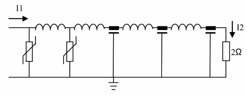
When testing the initial circuit, an injected 8/20µs pulse current, I1 in figure 2, of 2280A was reduced to a residual current, I2, of 256A in the 2 ohm load resistor. Subsequently, by carefully adjusting the filter components, the second stage of transient suppression was eliminated, and the circuit was further improved and simplified, resulting in a 65A residual current for an injected pulse current of 2360A.
Plots of the pulses measured on the improved circuit are shown in Figure 3.
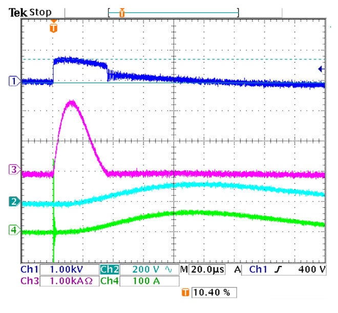
It is not easy to read across the laboratory 8/20µs pulse test results to the MIL STD E1 pulse because of the difference in energy content of the pulse, the non-linear behavior of the filter inductors, saturation of inductor core material, and parasitic capacitance of the inductors. However, for the 8/20µs pulse, a significantly higher residual current than 10A was expected due to the energy content of the pulse.
What was not certain was what value of residual current for the 8/20µs waveform would relate to the 10A requirement when testing with the proper MIL-STD E1 waveform.
Because there is no filter insertion loss requirement within MIL-STD-188-125, a standard design was developed to be commensurate with the MIL-STD-188-125 shielding attenuation requirement of 20dB at 10kHz and 80dB from 10MHz to 1GHz.
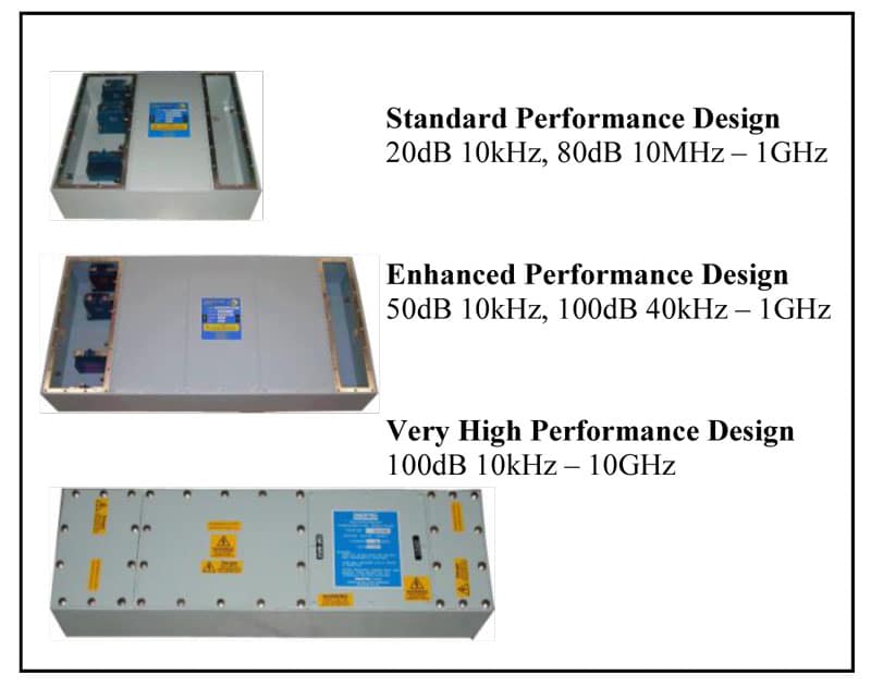
Accepting that there would be other applications requiring higher insertion loss to satisfy supplementary requirements such as EMI, two additional designs with higher insertion loss performance, were also developed. These designs are shown in Figure 4.
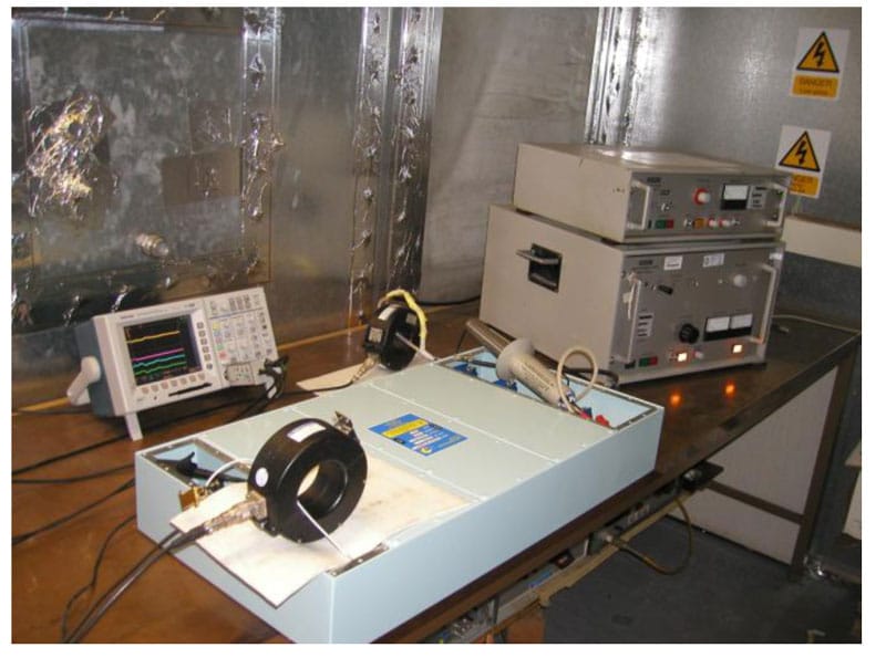
Figure 5 shows the test set-up of one of the three final designs in a screened test room in the MPE laboratory. The current and voltage monitoring probes and also the two pulse testers can be seen in the photograph.
After completing the filter designs and testing in the MPE laboratory, it was necessary to validate the designs by subjecting them to the correct MIL-STD pulses. This procedure is described in MIL-STD-188-125 as Acceptance Testing.
All three new designs were subjected to the correct MIL-STD E1 and E2 pulses at an independent test laboratory. This consisted of applying the E1 pulse at various current levels up to 2.5kA to check that the design worked over a range of pulse currents. The residual voltage was monitored along with the dI/dt (rise-time) and root integral (energy content) of the residual pulse. The circuits were then separately subjected to the E2 pulse. The insertion loss of the filters and varistor parameters were measured before and after application of the pulses as a check that the circuits had not suffered degradation as a result of either the E1 or the E2 pulse testing.
ACCEPTANCE TESTING RESULTS
All three designs were found to pass all tests very comfortably, being within the limits by a large safety margin. The most important parameter is the residual current and even the standard circuit achieved a residual current of less than 1.5A with a 2.5kA injected pulse, compared with the specification requirement of less than 10A. The results of the residual current for different applied peak currents can be seen graphically in Figure 6.
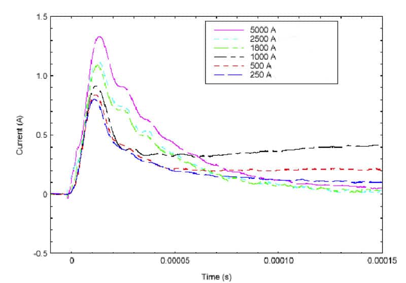
The residual currents are significantly better than those expected from a modified catalog filter. The higher performance circuits gave even better pulse performance than the standard design as well as offering a higher insertion loss.
The testing as described above was carried out on filters of 16A current rating. Further tests were subsequently carried out on a range of filter designs in current ratings from 6A to 200A, all of which passed the tests in a similar manner to the 16A filters. As the filter rated current increases, it becomes more difficult to achieve the residual current requirement. However, in all designs up to 200A current rating, a residual current lower than 4.5A was achieved providing a comfortable safety margin within the specification requirement.
CONCLUSIONS
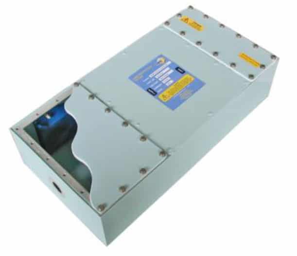
The final standard filter design, as shown in Figure 7, proved to offer an extremely low residual pulse current performance, much better than would be expected from an adapted catalog filter. This was achieved in a smaller and lighter package than would be possible for a modified catalog EMI filter. The circuit design also provided additional benefits of lower leakage current and lower heat dissipation compared to normal catalog EMI filters. The smaller size and weight provide benefits of ease of installation and a potentially more cost effective solution to HEMP protection.
Most EMP protection applications will benefit from such a design but the ones which will benefit the most are those where size and weight are critical parameters. These include mobile shelters, vehicles, telecoms cabinets, and Homeland Defense.
Applications which only need compliance with MIL-STD-188-125-1 or -2 can benefit from the small size and low weight of the standard circuit. Applications which need additional insertion loss performance to satisfy EMI, shielding or other requirements can still benefit from the good pulse performance of the new design philosophy with one of the higher performance circuits.
SUMMARY
A dedicated HEMP power filter design can give better pulse performance than an adapted catalog EMI filter and provide additional benefits in terms of size, weight, leakage current, power dissipation and cost-effectiveness.
REFERENCES
[1] MIL-STD-188-125-1 17 July 1998 “High-Altitude Electromagnetic Pulse (HEMP) Protection For Ground Based C4I Facilities Performing Critical, Time-Urgent Missions, Part 1 Fixed Facilities”
[2] MIL-STD-188-125-2 3 March 1999 “High-Altitude Electromagnetic Pulse (HEMP) Protection For Ground Based C4I Facilities Performing Critical, Time-Urgent Missions, Part 2 Transportable Systems”
Antoni Jan Nalborczykgraduated from Birmingham University with a BSc degree in Physics in 1973. He has worked for MPE Limited since 1979 and is currently Technical Director for MPE Limited in Liverpool, UK. Contact Jan at jnalborczyk@mpe.co.uk.
