
Introduction
In today’s world full of digital electronic devices, electromagnetic interference (EMI) is a major concern in both military and commercial marketplaces. Electrical equipment can become susceptible to these undesirable emissions and malfunction due to their presence.
The simplest and most cost-effective method for reducing EMI is to first attack it at the board level if possible. Given the increasing complexity of circuitry these days, it is rare that a printed circuit board (PCB) layout can solve EMI problems entirely; thus, board level shielding has become a requirement for most PCB designers.
EMI Basics and Board Level Shielding Design
Radiated EMI occurs when an electromagnetic wave travels in the direction of an electronic device and then disrupts the operation of that electrical component.
An electromagnetic wave consists of an electric field (E) and a magnetic field (H), and the ratio of E to H (E/H) is known as the wave impedance (Z). For air or free space, Zo = 377 Ω. An electromagnetic wave with an impedance below this value is predominantly magnetic, whereas a wave with an impedance above it is mainly electric.
Using a board level shield for EMI shielding means using a metal can, also known as a Faraday cage, to enclose an electronic circuit on a PCB. This in turn will limit the amount of EMI radiation from the external environment that can disrupt PCB components and also mitigate the amount of EMI energy generated by the circuit from escaping into the external environment.
The efficiency of a board level shield is measured in terms of shielding effectiveness (SE), which is the amount of EMI attenuation expressed in terms of decibels (dB).
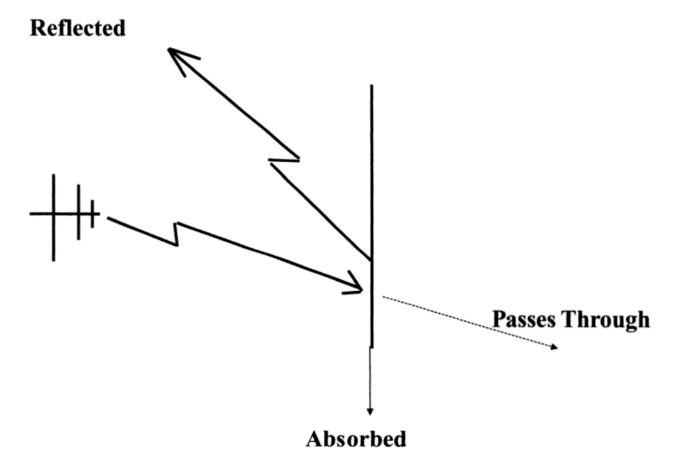
As depicted in Figure 1 (Gnecco, 2000), when an electromagnetic wave comes in contact with the shield material, some of that energy is reflected, some is absorbed into the shield material, and some of it passes through the material.
Thus, the total shielding effectiveness of an EMI shield is based upon the summation of the losses due to reflection and absorption.
Absorption loss is dependent upon the physical characteristics of the shield and is directly proportional to the thickness of the shield, relative magnetic permeability, electrical conductivity of the material, and the frequency of the electromagnetic wave.
Therefore, a thick-walled shield with high permeability and conductivity will perform well in terms of absorption loss. Absorption loss is critical when emission suppression is needed, such as when a shield is being used to prevent electromagnetic energy from escaping an enclosure; see Figure 2 (Tong, 2008).
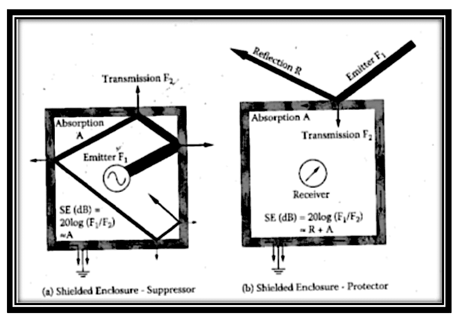
On the other hand, reflection loss is important when a PCB component is to be protected from external sources. Reflection loss is dependent upon the relative mismatch between the impedance of the electromagnetic wave and that of the EMI shield material.
If an electromagnetic wave’s impedance differs from that of an EMI shield, then the wave will be partially reflected back. On the contrary, if the shield’s and wave’s impedance values are closely matched, then the energy will pass through the shield.
It is important to note that electrically dominant incident waves (impedance greater than 377 Ω) have high impedance, and higher conductive metals have low impedance. Thus, highly conductive metals exhibit high reflection loss for electrically dominant waves.
However, for magnetically dominant incident waves that have low impedance (less than 377 Ω), the impedance mismatch between the shield and wave is minimal; hence, the resulting reflection loss is very low. As a result, absorption loss is critical for shielding magnetic fields.
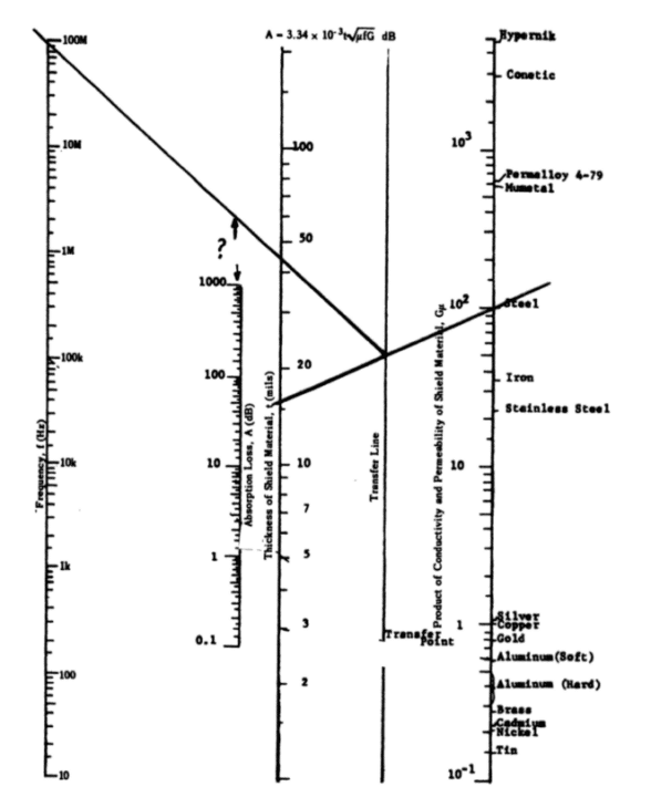
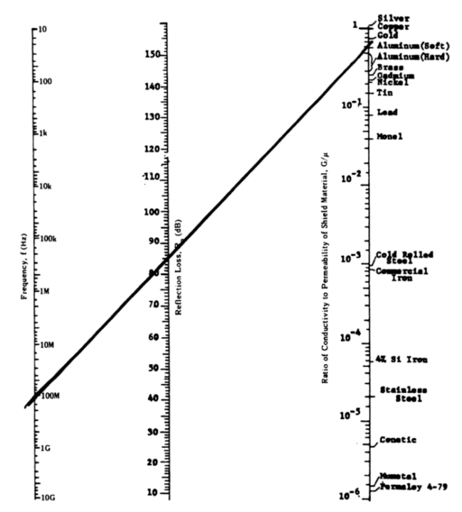
Figures 3 and 4 (Gnecco, 2000) illustrate the theoretical absorption and reflection loss that can be achieved with an EMI shield using different materials.
To use Figure 3, a line must be drawn from the known thickness of the EMI shield to the material being used, and then another line must be drawn from where it intersects the transfer line to the frequency of the incident electromagnetic wave.
It is evident when viewing Figure 3 that for a given frequency, a thick-walled shield with a high permeability material, such as high-permeability steel, will outperform a thin-walled, highly conductive shield made of copper or brass in terms of absorption loss.
On the other hand, Figure 4 reveals that for a given frequency, highly conductive materials (copper or brass) will surpass the performance of a lesser electrically conductive material (high-permeability steel or stainless steel) in terms of reflection loss.
Although conceptual tools such as Figures 3 and 4 are helpful in determining the appropriate shielding material for a given application, they do not account for apertures in the shield design.
The performance of EMI shields is greatly affected by seams and penetrations, especially when dealing with electrically dominant waves at higher frequencies. The higher the frequency of an electromagnetic wave, the shorter its wavelength and the more likely it is to escape through any openings in an EMI shield.
Therefore, when designing an enclosure, it is critical to minimize the apertures to decrease potential EMI leakage points and to maximize the quality of the design near apertures for overall performance and long-term reliability.
The frequency at which electromagnetic energy will propagate through an aperture without being attenuated is known as the cutoff frequency (fc).
- Frequencies above fc will propagate freely.
- Frequencies below fc are attenuated.
The equations below (Weibler, 1993) demonstrate how to calculate the cutoff frequency:
fc=c / λc ; where:
- c = speed of light (m/s)
- λc = cutoff wavelength (m)
- fc = cutoff frequency (Hz)
For:
- Circular apertures: λc=3.412r ; where r = radius of
the aperture (m); - Rectangular apertures: λc=2a ; where a = longest
dimension of the aperture (m)
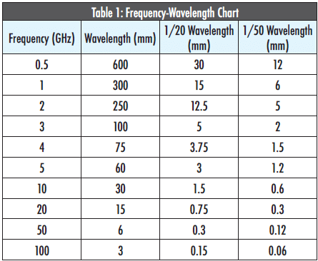
Besides knowing the cutoff frequency, a good rule of thumb to achieve excellent EMI shielding effectiveness in any application is to keep every aperture size no larger than 1/20 wavelength of the electromagnetic wave being attenuated and to aim for aperture sizes as small as 1/50 wavelength (Tong, 2008).
Table 1 below is a helpful resource that lists a sampling of frequencies, their corresponding wavelengths, and the recommended maximum aperture size based on 1/20 and 1/50 wavelength.
Proper design of EMI board level shielding is crucial, and if done right, it can even eliminate the need for overall enclosure-level shielding.
Many EMI shield manufacturers have fully tooled, standard, low-cost off-the-shelf options readily available. Therefore, it is a good idea to plan and design for the use of board level shields during the initial PCB design to take advantage of these options.
References
1. Gnecco, Louis T. 2000. The Design of Shielded Enclosures: Cost Effective Methods to Prevent EMI. Woburn, MA: Butterworth-Heinemann.
2. Tong, Xingcun Colin. 2008. Advanced Materials and Design for Electromagnetic Interference Shielding. Boca Raton, FL: CRC Press.
3. Weibler, Joseph. 1993. Properties of Metals Used for RF Shielding, EMC Test & Design.