Department of Computer and Electrical Engineering & Computer Science
Abstract
In the state-of-the-art wireless devices accommodating a dense layout of copper traces on the associated printed-circuit boards (single and/or multi-layered), is inevitable. Relevantly, considering the baseband level of audio and/or multimedia sections in smart handheld devices, ad hoc routing of traces, patterned zigzag on the printed-circuit board (PCB) often prevails; hence, a unique modeling strategy is required to address the extent of crosstalk victimization of trace-lines located proximally to the aggressing signal paths. Hence, the present study is devised to address and evaluate the performance integrity of a smart device with a PCB at the baseband section infested with a random cluster of traces; and, the associated high-speed digital transport on a trace (called aggressor) is assumed to induce unwanted crosstalk across victim traces in the vicinity. Relevant probabilistic attributes of randomly-dispersed trace patterns on the PCB invoking nondeterministic values of crosstalk are considered in this study; and, corresponding near- and far-end cross-talk (NEXT and FEXT) values are estimated. Such details can lead to compatible suggestions on crosstalk mitigation pursuits appropriate for baseband sections supporting high-speed digital transports. Results gathered from experimental studies are presented and corresponding theoretical estimates of NEXT and FEXT are cross-validated.
I. Introduction
The scope of this paper is to devise a method to evaluate the performance integrity of a smart handheld device having a printed-circuit board (PCB) at its baseband section, infested with a random cluster of traces [1-17]. The associated transport of high-speed signals (audio and/or multimedia) on a specific trace (called, “the aggressor”) and the corresponding high-speed digital signal-processing (DSP) would invariably culminate in causing unwanted crosstalk across nearby traces (dubbed as “victims”) commensurate with the associated electromagnetic (EM) coupling between the lines.
The probabilistic attributes of such randomly-dispersed trace patterns on the PCB invoke nondeterministic values of near- and far-end crosstalk (NEXT and FEXT) values in the victim traces [2] [4] [7-9]. However, knowledge on such parameters would lead to compatible suggestions and possible design-reviews concerning mitigation pursuits at baseband sections of smart handheld wireless devices.
In the present study, experimental studies are performed on a test PCB as well as the theoretical estimates of NEXT and FEXT are made and cross-validated with measured values. The theoretical heuristics proposed, computational effort exercised and experimental results obtained thereof are cohesively presented to portray the efficacy of the study and its usefulness. The paper is organized as follows: In the following section (SECTION II), necessary background details are furnished as regard to modern wireless handheld devices vis-à-vis the digital-signal transport characteristics at their baseband sections supported on a cluster of PCB traces. In SECTION III, an overview on the electromagnetic interference (EMI) across the random cluster of PCB traces is presented. Furnished in SECTION IV is a statement on the theoretical heuristics pursued along with descriptions on crosstalk estimation under discussion. In SECTION V, the inter-trace coupling factor (F) is defined and evaluated via EM field considerations. For analysis and computational study (and eventual experimental efforts), a test layout of PCB is described in SECTION VI. Presented in SECTION VII is the analytical framework pursued; and, lastly the measured and computed data are presented along with inferential details and suggestions on crosstalk mitigation in the context of the test PCB configurations.
II. Digital Signal Transport at Baseband Section of Wireless Handheld Devices
In modern context, the gamut of modern wireless devices supports a variety of diverse data applications (DDA) with outputs culminating in audio, video and alphanumeric displays. Specifically, considering the smart handheld devices in vogue, the terminal phase of information in such devices invariably refers to an infrastructure of screen-display and/or audio output [17]. These displays/outputs normally stem from a host of baseband-signal processed and conveyed via a densely-packed set of copper-traces routed on rigid and/or flexible PCB frames (single or multilayered) to the terminal sections of a touch-pad screen, loudspeaker and microphone devices. Thus exists between signal-processing electronics and final display-sections in handheld wireless devices are scores of transmission-lines manifesting as copper-traces that connect the source nodes and terminal points as necessary; and, these traces often meander randomly (to and from the sending and receiving ends). Furthermore, they are mostly packed to a very close extent with a format of parallel and/or nonparallel fan-outs often seen as two-dimensional (2D) routing patterns. Also, such traces may prevail on a single-layer PCB and/or they could be stacked across multiple layers as necessary.
Considering, the plan of layout and topology of traces on a PCB as outlined above, they could in general, be classified into two types: (i) They may represent a simple pattern with each trace being parallel to others, but all traces being highly proximal to each other. (ii) Alternatively, such traces though non-crossing, may denote a complex pattern with traces routed zigzag with no deterministic rule, but decided mostly on ad hoc based connectivity compatible for the required signal-flow. (In case, if some traces are required to cross each other, they would be kept separated layer-wise, by resorting to multi-layered PCBs).
Exclusive to baseband sections of handheld devices, the types of traces on a PCB described above are also required to support digital signal transports at very high bit rates. For example, with reference to state-of-the-art smartphones and other mobile/hand-held devices, the data bit-rates adopted at baseband levels could be significantly high (~ 500 Mbps); further, such streams of high-speed bits are often transferred between chips and/or various circuit nodes during baseband signal-processing, for example, between an image-sensor and an image sensor processor (ISP) [17]. To negotiate such transfers as mentioned earlier, an extensive count of copper-traces is envisaged at the board-level (formed either on a single surface or in multiple board/flex stacks). Further, these trace-lines could be of different lengths so as to accommodate the digital transits as necessary between the pins of any two devices placed at distinct locations on the board.
The physically transmitted baseband signal in essence represents a “digital-over-digital” transmission of pulse trains. In modern context of 3G through 4G considerations and associated LTE implications, the baseband data handled in the infrastructures of smartphones (as well as in similar devices) is relevant to specific versions of processors with chip-designs and/or system-on-chips (SoCs) that accommodate generous audio, and video digital signal-processing (DSP) schedules. Such processors are further required to meet multi-standard integration, reduced power dissipation and facilitate extra key-functions for the next-generation of smart, handheld devices. Relevantly, the associated baseband processors provide efficient operations with cost-effective, multimedia application-specific processing for the entry-level 3G as well as next-generation/evolving 4G systems.
In those complex baseband infrastructure and chip-specific operations mentioned above, the underlying applications invariably dictate the use of high-speed bit rates, which are placed on proximally located traces crowded and routed almost randomly as necessary. For example, considering video-processing support for 10/12 M-pixels imaging and 720p video-playback plus accelerated 2D/3D graphics, the operational needs push the processor speeds up to 1GHz or even higher. Concomitantly, related electrical transmissions of data point out the gravity of multiple high-speed transports on the limited-space circuit-board (and/or flexible-board) layouts. The underlying issue arising thereof can be summarized as follows: Together with the packaging designs of the components and chips placed on the board, the interconnections that support the said digital transports would invariably be in juxtapositions with close proximity; as well as, they could be routed and in transit unpredictably as necessary. Also, the transmission-lines (traces) deployed would occupy significantly of high density (per unit area) on the PCB and of varying lengths.
The digital transports in PCB contexts of baseband infrastructure described above often culminate in posing unique crosstalk issues that call for effective mitigations [4,9,12,14-16]. That is, considering the PCB layouts with the disposition of two or more adjacent lines closely spaced, the proximity of such traces as indicated earlier would lead to a strong EM coupling between them. That is, the EM forces caused by the time-varying signal transport on the traces would interact across adjacent lines leading to EMI. It amounts to crosstalk meaning unintentional transfer of signal waveform signatures from one-line (named earlier as the aggressor and also known as the infector) to neighboring lines (designated earlier as victims). Such observed crosstalk effects are largely decided by the extent of induced electromagnetic forces decided by relative signal voltage, v(t) and current i(t) entities, transported on the traces. Further, the traces depict a set of transmission-lines with distributed resistive, inductive and capacitive characteristics; and, the lossy dielectric characteristics of the circuit-board material supporting the traces will also play a role in deciding the EM propagation characteristics of the signal transmission implicating signal attenuation, as well as dispersive capacitive and inductive effects on the signal transported.
III. EMI on the Cluster of PCB Traces: An Overview
At system-level perspectives, a “trace” on a PCB refers to a transmission-line segment of an overall interconnection mostly comprised of a driver, the associated packages, one or two connectors plus vias etc. A typical wire-board package with traces fanning out is illustrated in Fig 1.
Predicting EMI proliferation on the PCB and the associated coupling behavior between the traces for the purpose of evaluating the resulting crosstalk is rather cumbersome especially, when the traces are arbitrarily off-set, laid non-parallel and randomly-spaced with respect to each other. Exact analytical solutions are not in general easy and mostly impractical. However, approximate modeling and deducing simulated results pertinent to simple, parallel topology of traces have been obtained in the past [10, 11].

Assessing crosstalk influence quantitatively becomes even more difficult when the signals traversing the traces correspond to high-speed digital waveforms with sharp rise-time characteristics. The corresponding inter-trace EM coupling and crosstalk may introduce time-interval-error (TIA) in pulsed waveforms due to spurious dispersion of EM energy, as indicated by the authors elsewhere in [17].
IV. Crosstalk Estimation: Statement of the Problem and Description
In view of the state-of-the-art aspects of crosstalk issues vis-à-vis PCBs exclusive to modern handheld wireless devices, the present study is indicated to address such problems pertinent to densely-packed traces on PCBs, when the lines are either parallel and/or laid out in zigzag patterns with the lengths of line-segments being of random values; further, all the lines are assumed to be designed so as to support high-speed, sharp rise-time pulsed waveforms, which are likely to cause significant EM energy dispersions [ 12, 17 ] in the composite PCB structure with metallic traces laid on dielectric board; and, the resulting pervasive electromagnetic interference (EMI) on the board would manifest as crosstalk in victim traces. The generic layout of a pair of traces on a PCB that encounter crosstalk problems as relevant to this study is illustrated in Fig. 2. The aggressor-victim pair need not imply parallel traces. In general, such pairs can be non-parallel as illustrated in Fig.3.


Further, illustrated in Fig.4 is a more comprehensive illustration of multiple victim traces {VT} infected by an aggressor, AT. In general, all such traces, may pose statistically undulating paths and as such, each trace can be characterized by a root-mean squared (RMS) value of undulation geometry observed on the 2D-plane of the PCB. Hence, shown in Fig.4 is a value XA of such RMS value for the aggressor, AT; and, the set {XV} denotes corresponding values for the victim set {VT}v = 1, 2, …. (Note: The victims are identified by the index, v = 1, 2, 3, …).

Commensurate with the scope of the present study outlined above, the underlying objectives aim at deducing a coupling index that would measure implicitly the induced electric (E) and magnetic (H) field components in the victim traces as a result of high-speed signal transported on an aggressor line expressed in terms of the time-varying voltage, v(t) and current i(t) functions. If the values of E- and H-field components are estimated, it is proposed here that they would implicitly allow inferring the associated EMI and hence lead to deducing the relevant crosstalk coupling coefficient of interest.
The traditional EMI and crosstalk modeling in such ambient would involve determining the inductive (L) and capacitive (C) effects perceived on the traces on the basis of reactive (mutual) impedance considerations [6]. However, in such L- and C-based EMI evaluation (and in relevant crosstalk estimation), the underlying estimates may become computationally intensive, inasmuch as the associated inductive and capacitive effects have to be ascertained (mostly numerically) across the extensive framework of grids within which, the victim traces and the aggressor are situated. In other words, the underlying inter-trace coupling when viewed in terms of classical inductance and capacitance considerations implies reactive influence (that is, voltage-current relational phenomenon in Kirchhoff’s sense) experienced across a huge number of distributed set of nodes and loops modeled on a two-dimensional grid depicting the 2D-pattern of meshes, each with characteristics transmission-line features of the traces involved.
However, as mentioned earlier, it is proposed here that the coupling index (F) of interest can be alternatively defined (in lieu of L and C perspectives) via the assessments of E and H field components across the framework of victim traces due to time-varying signal voltage and current entities. Corresponding coupling index (F) can be expressed as follows [18]:
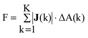
where |J(k)| denotes the magnitude of displacement current density (in A/m2) at the center of kth mesh of the matrix, K: [I ´ J] depicting the complete victim trace layout on the PCB.
![Fig.5 A matrix K: [I X J] meshes conceived on the 2D-plane of the PCB layout infested with victim traces](https://interferencetechnology.com/wp-content/uploads/2015/04/Figure5-300x290.jpg)
It is shown in [18], such an approach towards deducing EMI effects via equation (1) is as good as 98% of the results obtained by traditional capacitance-inductance estimation method. But, the advantages of using the approach via equation (1) are as follows:
• It is independent of the position of victim traces across the layout surface
• It is computationally less complex; (and, traditional finite-difference, finite-element or moment method (FDM, FEM and MM methods) can be adopted to determine numerically the associated E- and H- components of the interference leading to the estimation of the coefficient, F
• It is highly suitable for the random pattern of the victims versus aggressor lines; and, details as regards to exact dispositions of Kirchhoff’s nodes and loops deciding the [L] and [C] are not per se, required [19-21].
In view of the above, the present study is focused on deducing the coefficient (F) via E- and H-field components so as to specify the near- and far-end crosstalk (NEXT and FEXT) implications experienced in a typical complex trace-pattern, for example, as illustrated in Fig. 5. The notions of [18] and equation (1) are used, but significantly modified in this study specifically focused on PCB layouts of handheld wireless devices.
The crosstalk-induced coupled currents on the victim lines manifest as NEXT and FEXT. In a simple pair of parallel traces (with matched terminations), the aggressive (driven) line (1) would electromagnetically couple with the victim (un-driven) line (2), via two EM considerations namely, (i) the Columbic force field due to charges on the lines (traditionally implied as capacitive (C) effects); and, (ii) Faraday’s induction force field due to time-varying magnetic coupling between the lines, commonly regarded as inductive (L) effects. A pair of inductance and capacitance (m × n) matrices is normally indicated to analyze the underling EMI. For example, in the case of an aggressor-victim pair of lines (1 and 2), relevant L-C matrices can be written as follows [19-21]:
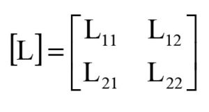
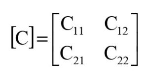
where L11 or L22 implies the self-inductance (henry per unit length) of lines 1 or 2 ; and, L12 or L21 line denotes the mutual inductance (henry per unit length) between the lines, 1 and 2. Similarly, C11 or C22 depicts the self-capacitance (farad per unit length) of the lines 1 or 2 (measured with respect to ground) and C12 or C21 is the mutual capacitance (farad per unit length) between the lines 1 and 2 per unit length. Correspondingly, the near- and far-end crosstalk voltages induced can be written as follows:


where vs is the source voltage impressed on the aggressor line (Fig. 2); and, l is the length (in m) of the trace-lines; further tr is the rise-time (in s) of the input signal, vs(t); and, l(L11C11)(1/2) denotes the propagation delay (in s) encountered along the line of length, l meters.
V. Inter-trace Coupling Factor (F) Estimation via EM Field Considerations
In lieu of the traditional way of estimating the inter-trace coupling coefficient in terms of L and C considerations indicated above, as mentioned earlier the present study is devised to formulate an alternative approach based on EM field parameters to deduce the crosstalk related coupling across PCB traces. It is surmised that the proposed method is more appropriate for randomly patterned traces. Relevant underlying heuristics are as follows: Consider a PCB layout with a victim trace (VT) and a noise (aggressor) trace (AT) as illustrated earlier in Fig.2. The crosstalk coupling between VT and AT is decided by an EM emission map overlapping VT and AT across the domain in a layout on a two-dimensional plane layout.
The traces (VT and AT) on the PCB in practice can be represented by segments joined up by a set of turning-points (Figs. 3 and 4). The number of such turning-points (N) and their locations on the PCB would depend on the electronic interconnections required as necessary. The coordinates of these turning-points are however, known a priori and therefore, deterministic. That is, they represent locales with defined coordinates on the 2D geometry of the PCB layout designed. Further, the terminal points (two for VT and two for AT) of the traces are also deterministically specified at known (predefined) coordinates; and, in general, all traces are assumed to be of same width (w meters). Given the trace details as above, the study in hand has the following motives:
a) To determine the E- and H-field components of the EMI on the trace domains of interest and knowing these components at the defined locations of turning-points
b) To calculate the overall resulting coupling index, F for any specified victim trace with respect to an aggressor trace
c) To assess the corresponding NEXT and FEXT levels at the terminal nodes
d) To verify experimentally the theoretical heuristics proposed and computational assessments made
e) To seek and suggest methods to mitigate (reduce) the crosstalk coupling involved
VI. Test PCB Layout for Analysis, Computational and Experimental Study
To illustrate the method of assessing the NEXT and FEXT for a random pattern of trace layout, the test PCB plus the overlaid traces on it considered is shown in Fig. 5. Suppose the traces as shown are such that the victim traces are laid to join fixed terminals {P1}, {P2} and such traces are assumed to be confined within a certain rectangular area. The aggressor trace is sourced by vs(t), normally a high-speed pulsed voltage, that produces EM-field components extended into the vicinity and invades the entire domain of victim traces.
The objective of the study is as follows: (i) To analyze the associated electromagnetics and infer the E- and H-field components specifically at the turning-points of interest; (ii) to assess thereof, the NEXT and FEXT levels in any given victim trace; and (iii) hence, to realize eventually a layout of victim traces with minimized NEXT and FEXT levels as an EM compatible alternative to the original PCB design. In addition to a typical aggressor versus victim pair node-to-node EM coupling illustrated in Fig. 6, possible examples of victim traces positioned between start and end nodes, P1-P2 with varying number (N) of turning-points are shown in Fig.7.


The layout (a) n Fig. 7, with the victim (P1 – P2) having no turning-points is taken as the reference and assuming the standard case of parallel traces, the NEXT and FEXT can be deduced deterministically via coupling matrix relations of equations (2) and (3). That is, in terms of [L] and [C] of equation (2), the following EM-field relations can be written toward inductive (IC) and capacitive coupling (CC) influences:

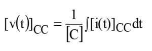
where vIC and vCC are voltages induced on unit length of the victim due to inductive and capacitive effects respectively. Corresponding relations written in terms of magnetic (H) and electric (E) fields are given by:


Hence, the net superimposed coupled EM-field relation is given by:

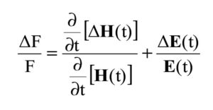
Suppose the turning-points (nodes) on the victim trace appear randomly located with respect to the aggressor trace so that, for a given set of [L] and [C]. The corresponding E- and H- components can then be specified as perturbed entities along the test traces. The fractional change in coupling influence thereof can be written as follows:
VII. Analysis
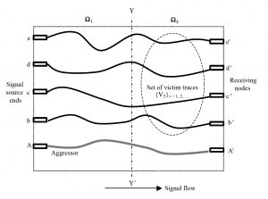
Consider the total space (W) of PCB layout wherein, as indicated earlier there could be a number of traces routed randomly on ad hoc basis, but placed proximal to each other. For example, a hypothetical layout on a given single layer is illustrated in Fig. 8 (where no physical crossings are assumed to be present).
Suppose AA’ denotes the aggressor (infector or driven trace) supporting a trail of high-speed binary information along time-scale. Let YY’ be a vertical line-of-separation on the PCB assumed to bifurcate the domain W into two regions, W1 and W2 denoting the near- and far-end sides respectively as shown. With reference to the spaces W1 and W2, and in terms of classical reactive coupling heuristics, each space has its own capacitive [C] and inductive [L] coupling matrices. These matrices can be alternatively viewed via electric (E) and magnetic field (H) components that emanate from the common aggressor line AA’ and interfering on (or placing crosstalk into) the set of victim lines bb’, cc’, dd’ etc. That is, relevant to W1 and W2, the capacitive and inductive couplings can be implicitly specified in term of the associated E– and H-field components respectively by a set of matrices as follows: and .
Correspondingly, each of W1 and W2 can be attributed with certain levels of susceptibility, S1 and S2 respectively to crosstalk on victims as a result of EM excitation stemming from the aggressor trace, AA’. In other words, the EM-field induced due to the signal-flow in AA’ (aggressor) will cause a trail of susceptance to EMI point-by-point on the victims; and, relevant values can be denoted as {Si}1 and {Sj}2 respectively in W1 and W2 as shown for example, in Fig.9, assuming an exclusive scenario of the victim bb’ versus the aggressor AA’.
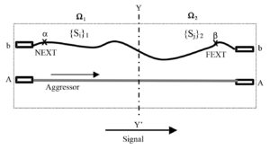
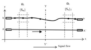
For the purpose of analysis, the domains W1 and W2 in Fig. 9 are further divided into grids (meshes) as illustrated in Figs. 10 and 11. Further, specific to the domain W1, the coordinate of a mesh is (xm = 1, 2, …, M, yv = 1, 2, … ). Likewise, for the domain W2, the coordinate of a mesh is specified as: (xn = 1, 2, …, N, yv = 1, 2, … ). And, the interfering field vectors E and H are assumed to vary mesh-by-mesh along x and y directions, point-by-point. Therefore, considering, the nodes representing the grids in the matrices of W1 and of W2, each node can be prescribed with a crosstalk susceptibility value (Sm)1 and (Sn)2 in W1 and W2 respectively. Further, the presence of {Sm}1 and {Sn}2 are denoted for example, as point-by-point values on the victim trace bb’ in Fig. 10 with respect to the aggressor AA’.
Therefore, considering the nodes at the extremities of the victim bb’, when m = 1 (in W1), {Sm = 1}1 denotes the NEXT; and, when n = N (in W2), {Sn = N}2 refers to the FEXT. Further, the elements of {Sm} and {Sn} are taken as normalized values (between 0 to 1); and, the normalization is done with respect to the signal (or EM-field) level enforced (by the signal) at the sending-end of the aggressor line. In moving along the victim line (say bb’), the step-by-step one-dimensional spatial progress of crosstalk influence (from mesh-to-mesh) can be specified by the associated randomness of EM-field influence (interference) on the victim. Relevant heuristics are as follows:
within each mesh of the matrix drawn on the 2D-plane of victim layout

and 2 respectively. (The victim traces are denoted by the index v both in and as identified in the text).
Considering the 2D framework of victim traces on the PCB, as indicated earlier, the media-line YY’ divides the 2D domain into two sections, W1 and W2 corresponding to the NEXT and FEXT regions respectively. Further, these sections are divided into mesh sets of {m ´ v} and {n ´ v} meshes as illustrated in Fig.11.
Each node corresponds to a mesh, where the EMI-based E- and H-fields induced render the nodes susceptible for crosstalk. The EMI coupling influence across the traces and the resulting susceptibility at each node to crosstalk is specified by (Sm, v)1 and (Sn, v)2 for the domains W1 and W2 respectively.
Considering an mth node in W1 and an nth in W2, the EMI coupling-influence proliferating (along such nodes in the row) conforms to a Poisson process; and as such, the dynamics of susceptibility values at (m + 1)th and (n + 1)th nodes can be written in terms of corresponding values at mth and nth nodes can be expressed as step-by-step proliferation as follows:
![]()
![]()
where l is a field-decay constant along the row (that is, x-direction and t is the instant of occurrence of the interference).
Similarly, the progress of EMI coupling along the column of meshes (in the y-direction, that is along the meshes at (v = 1, 2, …)th locations can also be written in terms of a Poisson process dynamics. However, the x- and y-directed coupling events can be regarded as two independent spatiotemporal processes over the 2D-neighborhood in question. Hence, the dynamics of the susceptibility index (S) assumed as a random variable can be written in terms of the following two independent stochastic, partial differential equations. With the coordinates of nodes designated as (xm, yv) and (xn, yv) for W1 and W2 respectively, relevant equations are as follows:
Along the x-direction:
![]()

And, a similar pair of partial differential equations can be specified for y-direction also. In equation (9) G denotes the spatial proliferation rate of EMI and h is a local coefficient that weights the newly perceived EMI coupling of (m + 1)th or (n + 1)th node due to the dynamics of proliferation.
The aforesaid differential equations refer to logistics growth models for the spatiotemporal evolution of EMI-induced susceptibility levels at the nodes considered. Relevant solutions assume the sigmoid format. That is, the susceptibility levels implicitly denote corresponding probabilities of EMI prevailing at the nodes along the grid; and, they can be written as sigmoidal solutions of equation (9) as follows [17] [22, 23].


where q is the fraction equal to the ratio of the fractional node population in W1 with respect to the total nodes across the entire framework of W1 and W2.; that is, q = (Number of nodes in W1/Total number of nodes in W1 and W2).
The aforesaid notions and results can be arrived at by following the probabilistic-theory of uncertainty applied to the random invasion of crosstalk proliferation in the domains of interest. Relevant outline is as follows: Proportion of net EMI-induced influences in the regions W1 and W2 can be deduced on the basis of statistical uncertainty of the EM coupling involved across victim traces due to the signal transits of the aggressor line. Given that the finite number of total nodes in the entire framework of W1 and W2 is mT and those victimized are (m1, m 2, m3 … etc.) with distinct susceptibility levels 1, 2, 3,…etc., the resulting statistical extent of uncertainty (q) of EMI coupling in W1 and W2 can be written in terms of the associated entropy (z) considerations expressed in Bernoulli forms as follows [24]:
Referring to W1, corresponding z1 along x-direction can be specified via entropy functional as follows:
For the region 1
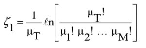
Likewise, for the region 2,

Therefore, q indicated above would correspond to the ratio z1/z2 of relative uncertainty (of EMI influences) associated in the regions W1 and W2; and, z1/z2 approximately reduces to, q = (Number of nodes in W1/Total number of nodes in W1 and W2).
Correspondingly, relevant to the randomness of trace-layout, the following (normalized) coefficients (0 to 1), RN and RF can be attributed to NEXT and FEXT in the vth victim of W1 and W2 respectively consistent with the relations in equation (10):

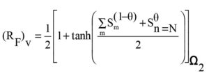
The concept of deducing NEXT and FEXT specified by equation (12) via probabilistic attributes of crosstalk susceptibility at the nodes of interest implies the following: The logistic functional aspect of equation (12) suggests that the pervasion of crosstalk along the nodes of a victim trace would increase (or decrease) as the level of susceptibility of coupling due to E– and H-fields on the victim (emanating from the aggressor) increases or decreases. Further, the statistically-implied gross influence of susceptance in W1 and W2 results from the superposition of such influences at the nodes {m} and {n} of W1 and W2 respectively.
As stated earlier, in classical perspectives of EMI estimation, the extent of overall EMI susceptibility is decided by EM coupling expressed via [C] and [L] deduced in a deterministic framework in terms of current-voltage based impedance relations (in Kirchhoff’s perspectives). In contrast, the present study follows the associated statistical attributes dictated by random perturbations of the values in the matrices [DE] and [DH] corresponding to the victim nodes of interest. As mentioned before, such randomness is largely imposed by the stochastic aspects of the geometrical layout due to random routing and/or geometrical spacing between the aggressor AA’ and the victim bb’ illustrated for example, in Fig.3. When the inter-trace coupling is viewed in terms of EM-field components, it can be quantified by the factor F deduced using E and H related entities and their relative perturbed values (caused by randomness) across the test area. That is, the invasion of E– and H– field components from the aggressor on the victims is assumed to cause corresponding random perturbations of coupling observed via differential values of [DE] and [DH] components; and, the result would be the crosstalk parameters manifesting as probabilistic values specified via equation (12 ).
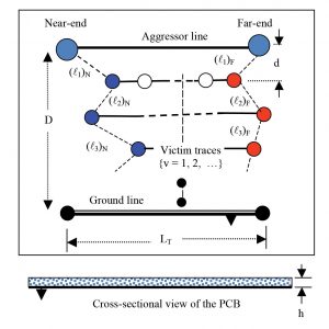
Hence considering the transfer of signal across the traces (endorsing undesired crosstalk coupling), it can be viewed in terms of relative EM-field components (specified implicitly via F) line-to-line (starting from the aggressor line) along the set of victim traces, {v = 1, 2, …}. Further, in terms of E and H related entities, relevant F-values can be prescribed using the geometrical parameters depicted in Fig. 12.
With reference to the geometrical entities of Fig. 12, the induced EM-field coefficients (0 to 1) in the vth victim trace would depend on the dimensions of the traces and the PCB. Further, the pervading field components (having three degrees of dimensional freedom) would decay with increasing distance of the victim trace from the aggressor. Correspondingly, the following EM field-dependent coefficients can be prescribed [ ] respectively for NEXT and FEXT evaluations (Fig. 12):
![]()
![]()
where ts denotes the settling-time of the pulsed signal. It is approximately equal to, (2 to 3) × (rise-time of the pulse, tr). Further, vN represents a reference voltage equal to 1 volt and vs is the applied signal level at the source-end of the aggressor trace.
In addition, the FEXT is also influenced by the propagation delay due to the finite distance from the source to the end-node along the aggressor line (of length LT m). Corresponding weighting coefficient on the FEXT can be written as follows:

Further, depicts the velocity of pulse transit on the trace and it can be specified via transmission-line concepts as nearly equal to, c/(er)1/2 where c (= 3 × 10⁸ m/s) represents the velocity of propagation of EM wave in free-space and er is the dielectric constant of the PCB substrate material. Hence, the final expressions for the NEXT and FEXT in the vth victim are respectively as follows:


VIII. Computed and Measured Results and Inferential Remarks
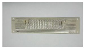
In order to verify the efficacy of the analysis presented and predictive formulations derived for the NEXT and FEXT concerning the test PCB under discussion, a test PCB illustrated in Figs. 13a and 13b is used and the aggressor line marked is excited with pulsed signal at two test frequencies, namely, 40 MHz and 80 MHz. Both the aggressor and the victims are terminated with the impedance of Ro = 50 ohm; and, the source impedance (RS) is also equal to 50 ohm.
With a known signal voltage vs (t) at 40 or 80 MHz applied at the aggressor source-node, the resulting (induced) near-end and far-end crosstalk voltages, namely, (uN)v and (uF)v respectively are measured using a broadband oscilloscope. Corresponding NEXT and FEXT values in the victims v = 1, 2, …, 8 are determined respectively as: (uN)v/vs and (uF)v/vs.

Further, using the board and trace details of the test PCB, relevant computations on NEXT and FEXT values as given by equation (15) are performed. Presented in Table 1 are relevant measured values and computed data on NEXT and FEXT observed at the set of victim traces (indexed as v = 1, 2, …, 8) and marked in Fig. 12. These details are also illustrated in Figs. 14a and 14b along with estimated statistical upper (UB) and lower (LB) bounds. These bounds denote the extrema that specify the error-bar on the estimated random entities (depicting the NEXT and FEXT values in question).
The UB and LB values are determined by replacing the tanh(.) function of equation (12) by Lq(.) where Lq(.) denotes the Langevin-Bernoulli function given explicitly by the following expression: Lq(z) = (1 + 1/2q) × coth[(1 + 1/2q)z] − (1/2q) × coth[(1/2q)z]. Here, the parameter q depicts the statistical disorder function [22]. That is, when q = 0.5, it refers to the condition of statistical disorder deciding the upper bound on the randomness of the estimates; and, when q = ∞, it denotes a state of total disorder prescribing the lower bound on the estimation. The concept of evaluating UB and LB values pertinent to the statistical estimates as above is described elsewhere in [23] by one of the authors.


MHz. (MV: Measured values and UB and LB denote the upper and lower bounds respectively of the computed data)
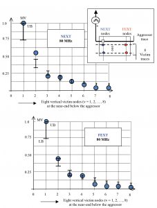
MHz. (MV: Measured values and UB and LB denote the upper and lower bounds respectively of the computed data)
From the results obtained, the following inferences can be made:
From the results obtained, the following inferences can be made:
- In lieu of the traditional method of using LC parameters to assess NEXT and FEXT values in a PCB supporting multiple traces intended for the transport of high-speed pulses, proposed here is an alternative, implicit technique based on evaluating the inter-trace coupling caused by E– and H-field components of the EMI involved
- The proposed method is comprehensive to include the statistical aspects of high-density traces laid out with random routings on the PCB. Such configuration of traces are common in the baseband sections of modern ha (xm = 1, 2, …, M, yv = 1, 2, …, ) handheld wireless devices
- Considering three attributes of the associated EMI phenomenon, namely, (i) EM field, (ii) statistical aspects of the physical PCB constituents and (iii) the transit delay issues of the signal pulse propagation on the traces, a pair of closed-form algorithms are derived (equations 15(a) and 15(b)) to deduce approximate values of the NEXT and the FEXT on a test PCB. Using the details and data as required, relevant computations of NEXT and FEXT can be done via simple computational effort. This is viably demonstrated with reference to a test PCB
- The efficacy of the algorithms developed is ascertained by cross-validating the computed details vis-à-vis measured data on a test PCB. The results presented in Table 1 and in Figs. 14(a) and 14(b) thereof indicate that the estimation procedure on NEXT and FEXT as advocated in this study favorably yields results (specified within the binding upper- and lower-limits) close to the measured data
- The proposal narrated here is a motivated effort to alleviate the non-prevailing status of a comprehensive method available to determine the NEXT and FEXT coefficients pertinent to the test PCB described infested with a random layout of traces. That is, with the advent of PCBs required to possess a high-density of traces with random signal transit paths as well as supporting high-speed pulses of DDA category (as warranted in modern wireless handheld devices), estimating the associated inter-trace EMI coupling and crosstalk efforts is imminent; however, no straightforward theoretical and/or computational strategy appears to be in vogue (to the best of authors’ knowledge). As such, the present study is offered.
The study performed also provides some conclusive observations as regard to EMI and crosstalk infestation in the class test PCB described. Typically, the following may be noted;
• The crosstalk values (NEXT and/or FEXT) are decided not only by the traditionally known mutual proximity of the victims (as well as with respect to the aggressor) but also implicated by the number of turning points on each trace. Such turning points depict discontinuities on the transmission-line with corresponding distorted E- and H- field distributions pervasively coupling onto the nearby lines.
• The victim trace closest to the aggressor may suffer crosstalk effects intensely
• Not only the geometry of trace routes, the mutual disposition of turning-points nodes in the adjacent traces would decide the NEXT and FEXT level ( Figs. 3 and 7)
• The net effect of crosstalk is decided by the following: (i) Pervasion of E- and H- fields across the random traces; (ii) randomness of the geometrical layout of traces and (iii) signal pulse characteristics.
Considering studies on the practical issues in high-speed PCB designs [2, 4], relevant objectives culminate in deducing tangible solution towards EMI suppression and formulating EM compatibility (EMC) considerations toward crosstalk minimization [6-9, 12, 15 , 16, 25, 26].
Based on the observations in the present study concerning the crosstalk perceived in the test PCB (having a cluster of randomly displaced traces), the following are suggested toward possible crosstalk mitigation efforts:
• Design the PCB layout with optimally separated traces
• Minimize the number of turning-points nodes on the traces
• If a directional change is inevitable for a trace, possibly make the associated turn smooth, rather being abrupt
Crosstalk mitigation efforts should also be done concurrently with minimizing the TIA considerations elaborated in [17]
References
[1] C. R. Paul, Introduction to Electromagnetic Compatibility, John Wiley & Sons,
Inc., New York, NY: 1992.
[2] M. I. Montrose, EMC and the Printed Circuit Board: Design, Theory, and Layout Made Simple, IEEE Press, New York, NY: 1998.
[3] S. J. Hall, and J. McCall, High Speed Digital Design: A Handbook of Interconnect Theory and Design Practice, John Wilson & Sons, New York, NY: 2000.
[4] M.S. Sharawi: Practical issues in high speed PCB design, IEEE Potentials, vol. 23, (2), 2004, 24-27.
[5] W. C. Bosshart, Printed Circuit Boards- Design and Technology, Tata-McGraw-Hill Publishing Co., New Delhi, India: 1984.
[6] P. S. Neelakanta and D. De Groff: “Smart” shielding may modify performance to fit, EMC Technology, vol. 9(3), May/June 1990, 25-29.
[7] P. S. Neelakanta and A. Preechayasomboon: EMI in high-speed digital transmission networks, Part I, Compliance Engineering, vol. XVI(7), November/December 1999, 36-47.
[8] P. S. Neelakanta and J. Sivaraks: Mitigating EMI in high-speed digital transmission networks, Part II, Compliance Engineering, vol. XVII (2), March/April 2000, 34-47.
[9] S. Scearce et al: PCB Crosstalk Fundamentals and Strategy. Cisco White Paper- 2009
Available at: http://www.pcbcarolina.com/images/sscearce-xtalk-ipc.pdf
[10] L. R Arnaut, C. S. Obiekezie, and D.W.P. Thomas: Empirical emission eigenmodes of printed circuit boards, IEEE Trans. on Electromag. Compat. vol. 56, (3), June 2014, 715-725.
[11] P. Rajeswari, et al.: Comparative study of radiated emissin in various microstripline structures on printed circuit boards, International Journal of Science and Research , vol. 2(4) , April 2013, 2319-7064
[12] High Speed PCB Layout Techniques, Texas Instruments
Available at: http://www.ti.com/lit/ml/slyp173/slyp173.pdf
[13] M.H. Pong, C.M. Lee and X. Wu: EMI due to electric field coupling on PCB, Proceeding of IEEE Annual Power Electronics Specialists Conference (PESC 98), (17-22 May 1998, Fukodo, Japan) vol. 2, 1998, pp.1125-1130.
[14] Circuit Board Layout Techniques, Literature Number SLOA089: Excerpted from OP Amps for Everyone, Literature Number SLOD006A, Texas Instruments, 2008
Available at: http://www.ti.com/lit/ml/sloa089/sloa089.pdf
[15] Design for EMI, Application Note AP-589, February 1999. Intel
Available at: http://www.intel.com/design/pentiumii/applnots/24333402.pdf
[16] Z. Xu et al.: Crosstalk evaluation, suppression and modeling in 3D through-strata-via (TSV) network, Proceedings of 3D Systems Integration Conference (3DIC) IEEE International, (November 16-18, 2010, Munich, Germany), pp. 1-8.
[17] P. S. Neelakanta and A. U. Noori: Mitigating time interval error (TIE) in high-speed baseband digital transports: Design for delay compensation at baseband infrastructure of smart-phones using fractal dispersive delay-lines, Circuit & Systems, vol.(5), May 2014, 115-123.
[18] M. H. Pong, et al.: Reduction of crosstalk on Printed Circuit Board using Genetic Algorithm in Switching Power Supply, IEEE Trans. on Industrial Electronics vol. 48, (1), 2001, 235-238.
[19] L. B. Gravelle and P. F. Wilson, “EMI/EMC in printed circuit board-A literature review,” IEEE Trans. Electromag. Compt., vol. 34, May 1992, 109-116.
[20] W. Xin, et al.: Reduction of EMI by electric field method, Proc. IEEE 14th Annual Applied Power Electronics Conference (APEC ’99), (14-18 March 1999, Dallas, Texas), pp.135-138.
[21] E. Bogatin, “Design rules for microstrip capacitance,” IEEE Trans. Comp. Hybrids, Manufact., Technol., vol. 11, Sept. 1998, 253-259.
[22] P.S. Neelakanta and D. De Groff: Neural Network Modeling: Statistical Mechanics and Cybernetic Perspectives, CRC Press, Boca Raton, FL: 1994.
[23] P.S Neelakanta and R. Yassin: Information-theoretics-based technoeconomic forecasting: Application to telecommunication service Industry, Netnomics, vol. 13, 2012, 45-78.
[24] P.S. Neelakanta and Fong Ah Meng: Bioassay approach to prescribe safe-limits of exposure to nonionizing radiation in ecosystems”, Biometric J. vol. 24(1), 1982, 69-86.
[25] W. T. Huang, et al.: The optimal number and location of grounded vias to reduce crosstalk, Progress in Electromagnetics Research (PIER), vol. 95, 2009, 241- 266
[26] P. W. Chiu, et al.: The impact of guard trace with open stub on time-domain waveform in high-speed digital circuits, Proc. IEEE Electrical Performance of Electronic Packaging and Systems Conference, (EPEPS 2009), (19-21 October 2009, Portland, Oregon, USA), pp. 219-222.


