In the previous article of this series, we looked at some of the major noise considerations in different power regulator topologies. Noise from these sources eventually makes its way to other components, and it could interfere with other portions of a system. Depending on the types of components used elsewhere in the system, noise may be innocuous or it may cause a design to fail. At minimum, an understanding of the primary noise coupling mechanisms will help designers prevent or correct design defects that can lead to an EMI failure.
In this section, we’ll look more at the physical mechanisms by which noise will couple from a power system to other components and circuits in an electronic device. These same mechanisms govern noise transfer in other circuits that are not meant for power delivery, although many EMI design problems originate from the power delivery system in an electronic system.
FIELDS AND NOISE
Fundamentally, the electromagnetic field is responsible for carrying energy between different circuits. A designer should be able to identify how the electromagnetic field could couple between certain critical regions in a design, thus they can engineer the system layout to minimize noise coupling. Should noise coupling remain a problem in a design, a designer can apply targeted solutions to the problem if they can determine the coupling mechanism.
Common-Mode and Differential-Mode Noise
All noise is radiated from a design in two modes: common-mode and differential mode. Technically, every wire carries a differential-mode current and emits radiation. However, in the EMC world, we normally care more about radiation from common-mode currents because common-mode noise is much more intense than differential mode noise. The two are related: common-mode noise can induce currents that generate differential-mode noise, and vice versa. Conducted currents can create near field radiation (e.g., crosstalk between signal lines) as well as emit into the far field, and this radiation in either regime can induce conducted noise. These effects are entirely driven by the electric field and magnetic field.
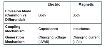
The table below summarizes the coupling mechanisms and generation mechanisms by which noise can be produced and received throughout an electronic system.

This table should be instructive as it relates a voltage/ current change in one area of a system to the noise received in some other area of a system. For example, in switched-mode power supplies, certain nodes experience high dI/dt events, and a nearby parasitic inductance will enable reception of lower frequency noise.
Similarly, nodes on switching FETs experience high dV/dt events, so parasitic capacitance can easily couple noise into a nearby circuit or conductor at higher frequencies. Capacitive coupling should be reduced around these nodes to prevent noise transfer via a displacement current in nearby structures.
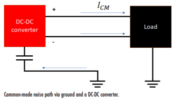
Parasitic capacitance is difficult to deal with and is one reason for common-mode noise coupling throughout a system. Common-mode noise in electronics, including PCBs or packages with multiple ground regions like a chassis, arises due to capacitive coupling around closed loops. Such capacitive coupling between one ground region and multiple conductors via a power system is a wellknown mechanism that allows noise coupling throughout a circuit.
In a system with an earth ground (PE) connection in the physical layout, it’s possible to create closed loops via the PE region and the power supply as shown in the image below. Some of this noise can propagate to an IO and possibly over a cable, later reaching a destination component. This is one reason a differential protocol might be used for data transfer, as well as the resilience against ground offsets when routed over long cable runs.

Why should this noise couple around the system at all? The answer lies in the fundamental behavior of the electromagnetic field.
Coupling Via the Electric Field
The electric field is related to the force that exists between electric charges. The strength of the electrical field is directly proportional to the potential difference between two conductors and is inversely proportional to their distance from each other. Essentially, this means that any two conductors separated by some distance between in a PCB or package will have some capacitance and can transfer energy between each other via the electric field.
If there is capacitive coupling that possibly leads to common-mode currents, it likely appears due to coupling between the nodes with highest voltage magnitude and/or highest dV/dt values. If you can identify these regions of the device, some steps can be taken to weaken coupling to nearby conductors and circuits.
Coupling Via the Magnetic Field
Magnetic coupling occurs due to induction as described in Faraday’s law. All currents produce a magnetic field, while a changing current produces a changing magnetic field. Since only changing magnetic fields can induce noise in other circuits according to Faraday’s law, DC currents will never induce noise in other circuits. Instead, it is the dI/dt nets and nodes in a design that will be responsible for coupling noise into nearby current loops via a changing magnetic field. The strongest coupling between two nets will occur in the following conditions:
- When the source current loop is parallel to the receiving current loop
- When the dI/dt value on the aggressor loop is maximized
A circuit can be shielded by enclosing it in high-µ material, although this method is complicated and expensive, and stops being effective above ~300 kHz. Magnetic field emissions can usually be controlled best when they are minimized at the source. In general, this requires the use of transformers and inductors designed to reduce radiated magnetic fields. It is also critical that the circuit board layout and interconnect wiring be designed to limit the current loops’ size, particularly in paths with high current.
CONCLUSION
With these noise conduction and emission mechanisms in mind, we can now start to think about some practical solutions to noise coupling in order to achieve EMC compliance in power systems and in their supporting circuitry. This can involve several techniques implemented in power supplies, embedded power converters, and many other designs that require noise suppression.
Once the particular source of the noise (both location and noise mechanism) is identified, it can often be suppressed in two possible ways:
- Locate and eliminate ground discontinuities in the PCB layout
- Identify areas with large current loops or close spacing between dV/dt nodes
- Strategically place filters with appropriate components
- Judiciously apply shielding in the design


