Alastair R. Ruddle, Ph.D., MIRA Ltd., Nuneaton, UK
Toroidal current transducers are widely used in EMC measurements, both for monitoring currents flowing on single cables or cable bundles and for injecting currents onto such cables or cable bundles. The latter forms the basis of a well-established approach to susceptibility testing (bulk current injection) that is used in the automotive and aerospace industries [1-2]. Induced currents are also monitored in certain immunity tests, such as those used in the aerospace industry [3]. Some methods for characterizing shielded cables employ both current injection and current monitoring transducers [4], while other possible applications are outlined in [5]. For current measurement purposes, these devices are calibrated in terms of their transfer impedance, which relates the current on the cable passing through the transducer to the voltage generated at its terminals. For current injection applications, these transducers are characterized in terms of insertion loss. The scope of this article, however, is limited to issues concerning the determination of transfer impedance for toroidal current measurement probes at high frequency.
CURRENT PROBE CALIBRATION FIXTURES
Current transducer calibration is normally carried out using a special calibration fixture, which is often provided by the probe manufacturer and can be used for both transfer impedance and insertion loss calibration. The calibration fixture essentially provides a short length of straight wire around which the transducer can be located and which terminates to coaxial connectors at each end. The shells of the coaxial connectors are connected by a simple metal structure that can accommodate the transducer. Typically this is a simple open ended box (i.e. a loop of four flat metal panels) enclosing the wire, which allows easy access to the transducer terminals at the open ends. In some examples, however, the interior is almost completely enclosed, with just a small aperture to allow a cable to be connected to the transducer terminals. Although some current transducers have solid bodies, with the result that the cable under test must be threaded through them, most are constructed with two hinged parts so that it can be more easily clamped around a cable. Nonetheless, the structure of the calibration fixture normally needs to be opened in order to allow the current transducer to be mounted around the wire.
At very low frequency the current flowing in the central wire will be the same as that measured or injected at the coaxial ports. At higher frequencies, however, impedance mismatches will result in interference between reflections and a standing wave on the internal wire of the calibration fixture. For these reasons impedance matching structures are often included to reduce the impact of these effects. Minimizing the length of the central wire also helps. However, these measures may not be fully effective, particularly at higher frequencies.
SIMPLE TRANSFER IMPEDANCE DEFINITIONS
The transfer impedance parameter is intended to provide a mapping between the current flowing in the cable passing through the current measurement probe and the voltage that appears at the terminals of the transducer.
The input connector of the calibration fixture is denoted Port 1, the output connector is Port 2, and the transducer output is Port 3. If the scattering matrix for the system with the current probe in the calibration fixture is P(ƒ), where ƒ is the frequency, then the voltage at the current probe terminals is:
(1)
where I0(ƒ) and V0(ƒ) represent the current and voltage incident at Port 1, |P31(ƒ)| is the magnitude of the frequency dependent transmission coefficient from Port 1 to Port 3, and ZC represents the characteristic impedance of the measurement system (which is assumed to the 50 Ω and frequency independent). The transfer impedance of the current probe as defined in [1], which is referenced to the input current, is then:
(2)
A better transfer impedance estimate may be obtained by using the current flowing out of the device as the reference current. However, the current transducer itself is also likely to have an impact on the system, suggesting two possible options for the reference current: the output current for the empty calibration fixture, or that with the probe present. The current exiting at Port 2 with the probe present is |P21(ƒ)|I0(ƒ), so using this as the reference current for the transfer impedance gives:
(3)
Similarly, if the current flowing out of the empty calibration fixture is used as the reference, the transfer impedance estimate is:
(4)
where J(ƒ) represents the scattering matrix for the empty calibration fixture (of order 2 x 2, as this has only two ports).
If the probe does not affect the system then P21(ƒ)=J21(ƒ) and the transfer impedances Z1(ƒ) and Z2(ƒ) are identical. Furthermore, if transmission through the calibration fixture is near-perfect, by careful impedance matching, then P21(ƒ)=1 or J21(ƒ)=1 and both Z1(ƒ) and Z2(ƒ) reduce to Z0(ƒ).
TAKING ACCOUNT OF JUNCTION REFLECTIONS
An improved estimate for the current at the center of the wire, taking account of interference between reflections from the coaxial ports, can be obtained using a simple 1D transmission line model to interpret the scattering matrix for the calibration fixture [6]. This analysis requires the phase, as well as the amplitude, for the frequency dependent transmission and reflection coefficients between the coaxial ports of the system, which can be obtained using a vector network analyzer.
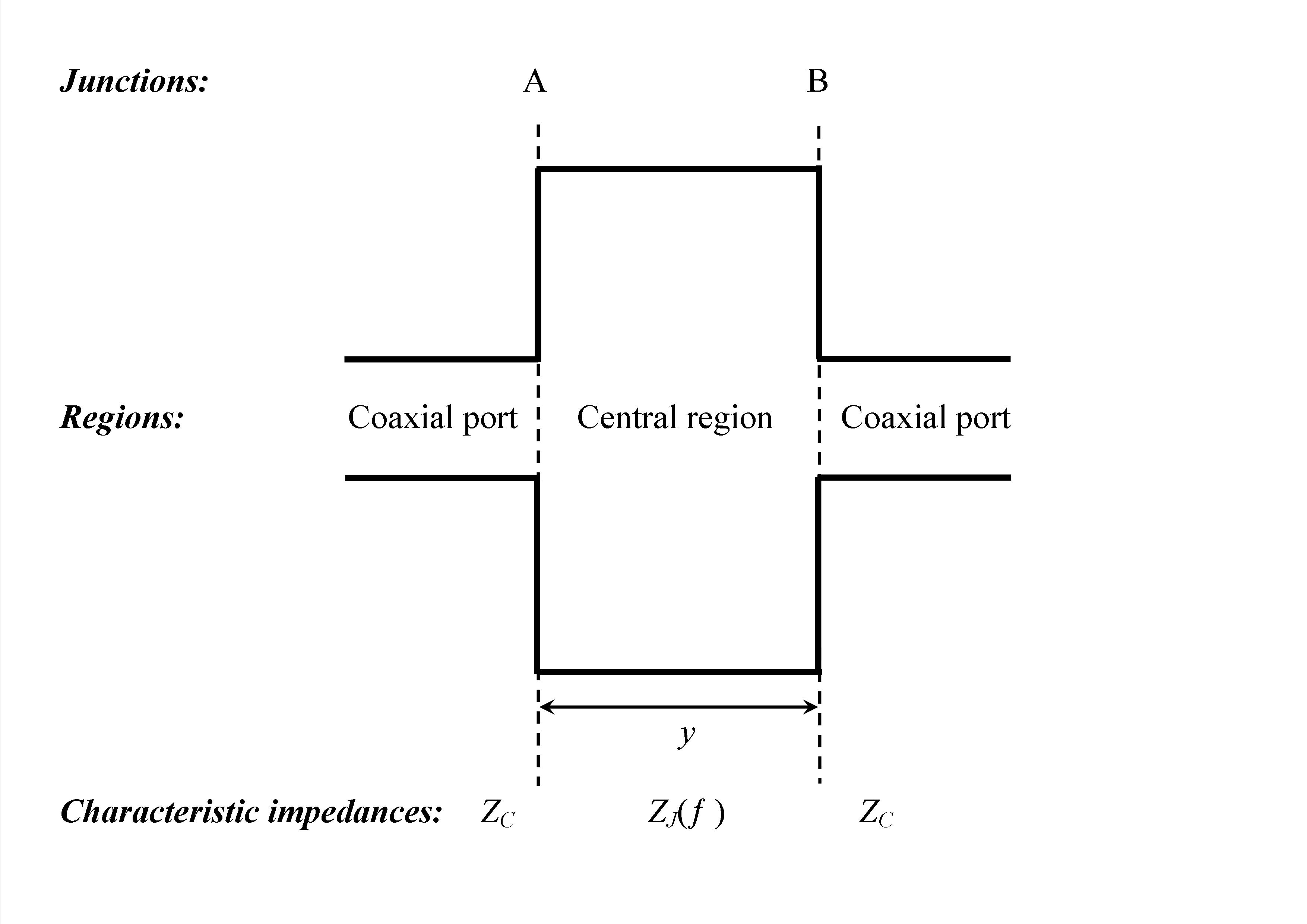
It is assumed that the calibration fixture may be considered as a section of uniform transmission line with characteristic impedance ZJ(ƒ) which is terminated at each end with identical transitions to the two coaxial ports of characteristic impedance ZC (see Figure 1). The junctions between the two types of transmission line will give rise to finite reflection coefficients and the resulting reflections will then interfere in a manner that depends on their electrical separation. This model assumes that the junction reflection coefficients take account of the additional path lengths that are introduced between the outer conductors of the coaxial ports as a consequence of the geometry of the calibration fixture.
It is assumed that the system is symmetrical and no energy is returned from the output port. Using the current at the center of the wire for the empty calibration fixture as the reference (i.e. at s=y/2), it can be shown [6] that the transfer impedance estimate taking account of the junction reflections is given by:
(5)
where ρ1(ƒ) is the reflection coefficient at junction A due to the abrupt change in impedance from ZC to ZJ(ƒ), β(ƒ) is the propagation constant in the empty calibration fixture, and y is the distance between the two junctions.
The parameters ρ1(ƒ) and β(ƒ) can be obtained from the complex components (both amplitude and phase of the reflection and transmission coefficients are required) of the measured scattering matrix J(ƒ) for the empty calibration fixture as follows:
(6)
(7)
The scattering matrix for the calibration fixture can therefore be used to determine the propagation constant for this structure, and hence the reflection coefficients at the coaxial ports. These two quantities are then sufficient to correct the transfer impedance for the effect of finite mismatches in the calibration fixture. The simpler approximations described in the previous section can also be derived from equation (5).
VALIDATION OF 1D TRANSMISSION LINE MODEL
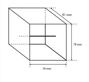
A 3D numerical model of a simple calibration fixture has been used to assess the validity and limitations of the approach described above. The inputs for the real device that was investigated have no special matching structures: the dielectric of the coaxial connectors is trimmed to be flush with the interior surface and the center conductors project through to connect with the central wire. The internal dimensions of this structure are illustrated in Figure 2, and the 3D numerical model was implemented using the transmission line matrix (TLM) technique [7]. In the model, the central wire was terminated with 50 Ω ports, and both the metal panels (≈3 mm thick) and the wire (≈2 mm in diameter) were assumed to be perfect conductors.
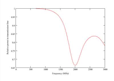
The scattering matrix for the modeled structure can be determined from the currents at the ports of the device. The sum of the power reflected at the input and transmitted to the output can then be used to establish where the assumption that the device is lossless begins to break down. It can be seen from Figure 3 that, for this structure, this is a reasonable assumption for frequencies up to about 1 GHz (where the loss is only 0.5%).
For this structure, the wire length corresponds to around 0.1 wavelengths at this frequency, while the dimensions of the larger plates are approaching 0.25 wavelengths. At higher frequencies the power lost through radiation becomes increasingly significant. Measurements can similarly be used to determine the frequency range over which a real structure can be regarded as lossless. The current at the center of the wire can be computed directly from the TLM model for comparison with estimates based on the port currents or derived from the computed scattering matrix for the system (as described in the previous section).
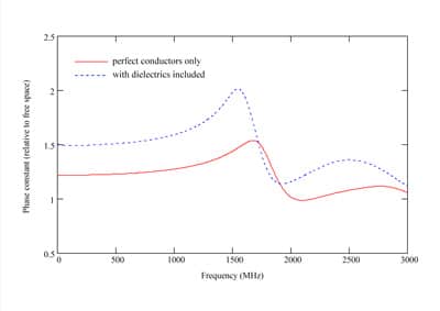
The real calibration fixture has thin layers of insulating material (≈1 mm thick) bonded to the inner faces of structure, and the central wire is surrounded by insulation (≈0.6 mm thick). The electrical properties of these materials are unknown and therefore difficult to model with any certainty. Results for the propagation constant estimated from the computed scattering matrix are illustrated in Figure 4, which is derived from simulations based on only the metal parts of the structure, and with representative dielectric materials added to the model (assumed to be lossless, with relative permittivity of 3 for the insulating sheets and 2.5 for the wire insulation).
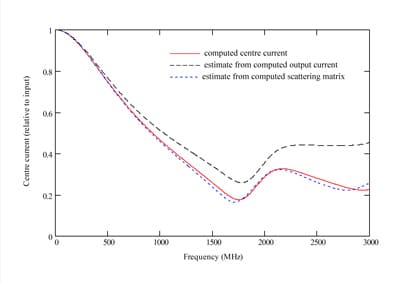
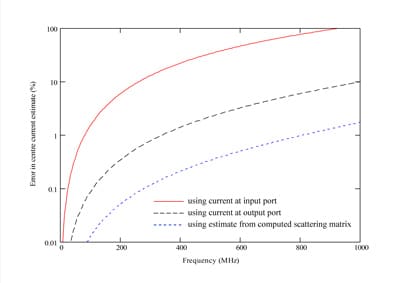
The values for the real component of β(ƒ) are greater than the free space propagation constant for the purely metallic case, and the effect of the dielectric material is to further increase this parameter. The imaginary components are zero up to about 1 GHz, where the behavior of the device is becoming more complicated. The results of Figure 5 illustrate that, although the current at the output provides a reasonable estimate for the current at the center of the wire for low frequencies, the value obtained from the scattering matrix for the device provides a much better estimate. Moreover, this method continues to provide a very good indication of the current at the center of the wire, even at much higher frequencies where losses become more significant. Although the structure begins to radiate at the higher frequencies, the junctions remain lossless and the transmission line model still provides a good estimate for the current at the center of the wire. The errors resulting from estimating the current by different methods are compared in Figure 6, showing errors of little more than 1% at 1 GHz for the proposed method, compared with around 10% for estimates based on the output current and much larger errors using the incident current.
INCLUDING PROBE FOR OVERSIZED CALIBRATION FIXTURES
If the probe width is sufficient to fill the calibration fixture then equation (5) could also be used to obtain a transfer impedance estimate relative to the current at the center of the probe by replacing J11(ƒ) and J21(ƒ) in equations (6) and (7) with P11(ƒ) and P21(ƒ). However, if the calibration fixture is wider than the thickness of the current transducer, the latter may then introduce additional mismatches when the calibration measurements are made. Although a transfer impedance estimate referenced to the current at the center of the empty calibration fixture is still possible in this case, another option could be to reference the transfer impedance to the current at the center of the probe partially filling the calibration fixture.
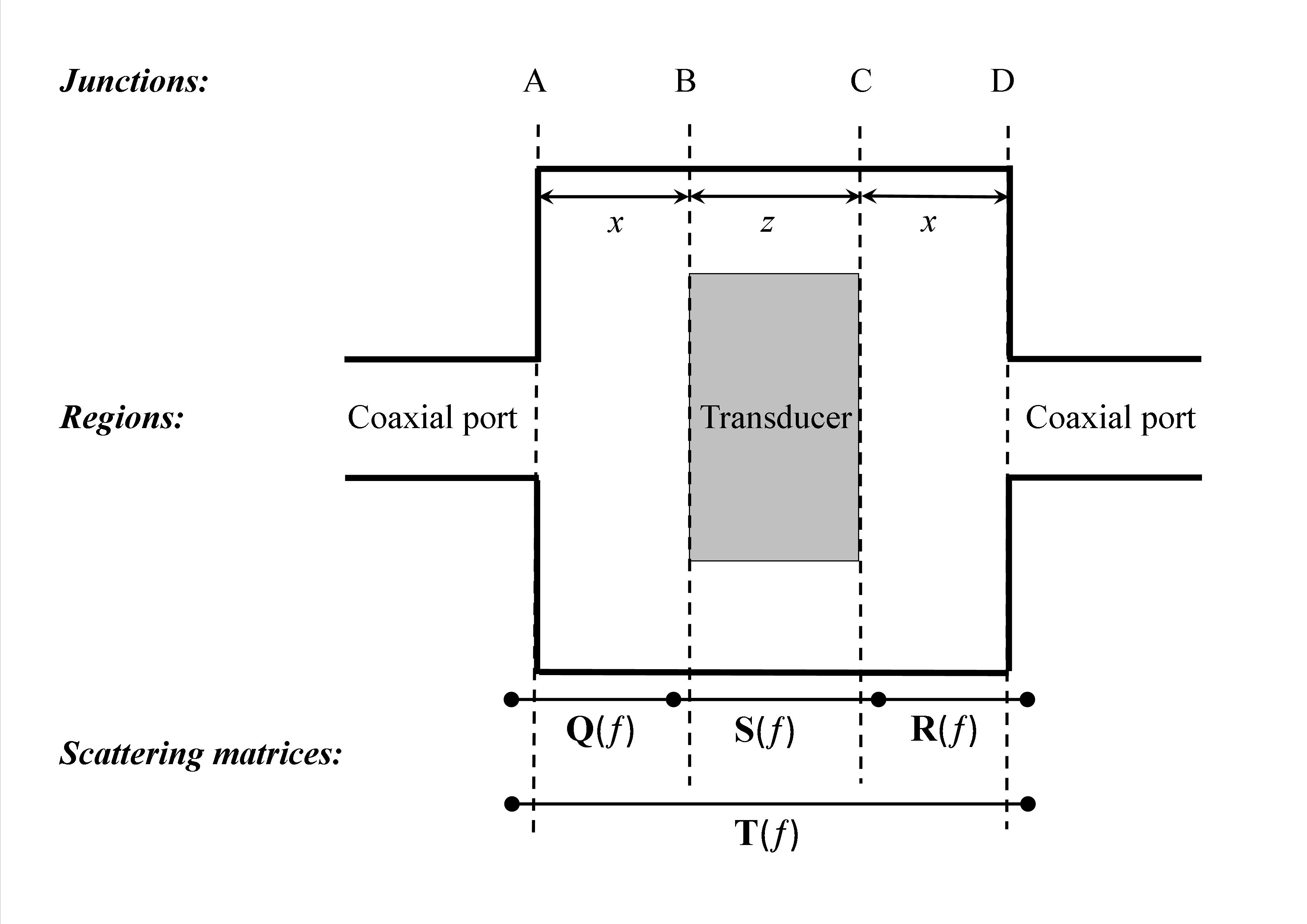
In cases where the transducer does not completely fill the calibration fixture longitudinally, the significance of the additional mismatches that are introduced by the transducer can be estimated using an extended 1D transmission line model as illustrated in Figure 7, in which there are now four impedance junctions and the region occupied by the current transducer is represented by the scattering matrix S(ƒ).
Assuming that the current probe is located centrally in the calibration fixture, the networks represented by matrices Q(ƒ) and R(ƒ) in Figure 7 simply comprise the junctions at the coaxial ports cascaded with transmission line sections representing the lengths (x) of empty calibration fixture on either side of the current transducer. Consequently, their scattering matrices can be described in terms of the parameters ρ1(ƒ) and β(ƒ), obtained from measurements of the scattering matrix J(ƒ) for the empty calibration fixture.
For this symmetrical network it can be shown [8] that the elements of the scattering matrix S(ƒ) for the probe region can be extracted from the measured scattering matrix T(ƒ) for the calibration fixture with the transducer positioned at the center of the calibration fixture, together with the parameters ρ1(ƒ) and β(ƒ) obtained for the empty calibration fixture. The scattering matrix for the device region can be de-embedded from that for the overall network using:
(8)
(9)
The region occupied by the current transducer, represented by the matrix S(ƒ), is again approximated as a symmetrical pair of lossless junctions separated by a length z of transmission line of propagation constant γ(ƒ). Consequently, the same analysis method used to extract the transmission line model for the empty calibration fixture can then be applied to the matrix S(ƒ) to extract the propagation constant γ(ƒ) for the transducer region and the reflection coefficients ρ2(ƒ) associated with the faces of the device. Thus, following equations (6) and (7):
(10)
(11)
The transfer impedance for those cases where the transducer does not fill the calibration fixture, using the current at the center of the transducer (i.e. at t=z/2) as the reference, can be shown [8] to be:
(12)
where the parameters a(ƒ) and b(ƒ) represent additional terms as follows:
(13)
(14)
NUMERICAL MODEL VALIDATION EXAMPLE
This investigation of current probe calibration methods was prompted by disparities found between numerical simulations and “measured” results. The measurements employed a small current transducer (25 mm in diameter and 16 mm thick). This device, therefore, did not completely fill the calibration fixture (illustrated in Figure 2), in which the central wire was 36 mm long. Consequently, the original simulation is used here to judge the success of the various calibration options.
A common test case used in the validation of numerical modeling techniques for EMC applications comprises a cavity containing a wire and an aperture that permits coupling with an external field. In such an experiment, the current at a point on the cable was recorded under external illumination from a log-periodic dipole array antenna in a semi-anechoic chamber. The chamber is 25.6 m long, 13.6 m wide and 8.8 m high, and is lined with a 1.8 m long twisted pyramidal foam absorber. It is used primarily for commercial radiated immunity testing of vehicles ranging in size from cars to industrial vehicles.
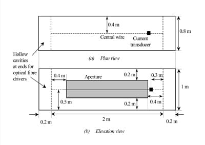
The object under test (see Figure 8 ) was a rectangular aluminum box with sides of length 0.8 m, 1 m and 2.4 m. One of the 1 m wide faces was equipped with a 1.2 m long, 0.6 m wide aperture that was centrally located. The interior cavity was 2 m long and contained a wire that was located along the longitudinal axis of the box and terminated with 50 Ω loads. The current transducer was placed at 0.3 m from one end of the wire. The cavities at each end of the box (0.2 m long) housed the cable terminations and an optical fiber transmission system linking the current probe to the data acquisition system.
The lowest face of the box was mounted at 0.8 m above the ground plane (using wooden trestles) and the face containing the aperture was vertical and illuminated by the antenna, which was aligned with the transverse axis of the box (see Figure 9). The center of the aperture was located above the center of the chamber. The longitudinal axis of the antenna was 1.5 m above the ground and the feed point was 1.5 m from the box.
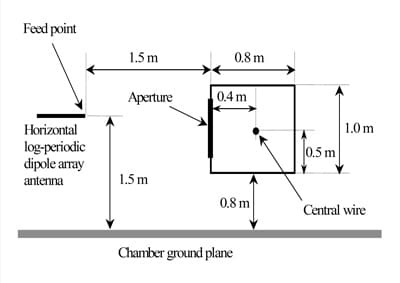
A 3D numerical model of this system was constructed using TLM. Both the measurements and the simulations included a preliminary “empty chamber” calibration in which the “threat” field at the point corresponding to the center of the aperture was determined. Measured and simulated results obtained with the test object in place may then be normalized to the corresponding threat field in order to obtain data sets that are directly comparable. This approach is useful for model validation purposes as it avoids the need to model the real antenna and its excitation in fine detail and also limits the effects of systematic errors in the field measurements.
Transfer impedance estimates obtained for the current transducer used in the measurements are illustrated in Figure 10, including all of the current reference options described above. The impact of the various transfer impedance estimates on the interpretation of measured currents from the model validation experiment is illustrated in Figure 11, which compares the current predicted from the TLM model with measurements that are calibrated using the various options described above.
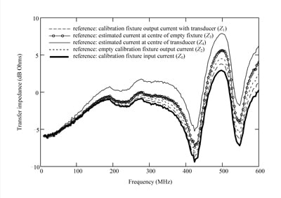
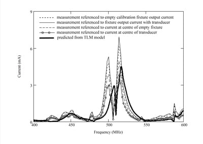 Comparing the results for the feature around 500 MHz, the measurement calibrated using the transfer impedance Z4 defined in equation (10), based on the estimated current at the center of the transducer during the calibration, is at almost the same level as the corresponding (but displaced) feature in the model results. The amplitude of the dominant feature (around 520 MHz), which is larger than the predicted value for the other calibration schemes, is smaller than the prediction for this case, but the overestimate for the feature that occurs at around 590 MHz is smaller than for the calibrations based on the calibration fixture output currents (with or without the transducer present) or the estimated center current for the empty calibration fixture.
Since the frequencies and relative magnitudes of the features in the measured and predicted current spectra are not identical, it can be expected that it will become increasingly difficult to judge the success of more refined calibration approaches. The disparities that arise can probably be ascribed to limitations of both the model and the measurement. The numerical model used for the validation experiment did not include any representation of either the current transducer or its associated coaxial cable (which linked the device to a bulkhead connector, and hence to an optical fiber transmitter housed in a cavity inside the test object). The log-periodic dipole array antenna that was used to illuminate the test object for the measurements was also too complicated to be represented in detail in the simulations, due to computational limitations at the time this work was carried out. In addition, the model neglected material losses, so predicted levels might be expected to be higher than in the measurements. Frequency shifts between similar features found in models and measurements are also routinely encountered in model validation experiments. Furthermore, the impact of the transducer on the wire that passes through it is unlikely be the same in the validation measurements as in the calibration measurements, and the influence of the transducer is not represented in the simulations.
Although referencing the calibration to the estimated current at the center of the transducer results in a lower “measured” current than predictions for the dominant feature, the overall results suggest that this approach provides a more satisfactory reference for the calibration in this example. In addition, it is expected that the predicted resonances may be slightly higher than the measurements due to the use of perfect conductors in the simulation.
CONCLUSIONS
A simple 1D transmission line model has been used to assess the impact of the reflections that occur within a calibration fixture when calibrating a current transducer, including the case where the current transducer does not completely fill the calibration fixture longitudinally. A number of alternative estimates for the transfer impedance of the current transducer have also been derived, based on referencing the transducer output to the current at different points in the calibration fixture, with and without the current probe present. The various currents that are used for this purpose are estimated from measurements of the scattering matrices for the calibration fixture under empty and loaded conditions using the 1D transmission line model.
The relative success of the various calibration approaches has been investigated for frequencies up to 600 MHz using measured and computed results from a model validation experiment. Measurements of the current induced on a wire inside a cavity backed aperture illuminated by a nearby log-periodic dipole array antenna in a large semi-anechoic chamber were reinterpreted using the various calibration options and then compared with currents predicted from a numerical model of this system.
The results from this analysis suggest that the output current from the oversized calibration fixture with the transducer in place does not provide a reliable reference for the transducer calibration. Using the output current for the empty calibration fixture as the calibration reference brings the measured measurements closer to the simulations for the validation experiment, and further improvements are obtained by referencing the calibration to the estimated current at the center of the empty calibration fixture. However, it is considered that a more reliable estimate for the transfer impedance of the current transducer is achieved by referencing the transducer output to the estimated current at the center of the transducer during calibration using an over-sized calibration fixture.
Other approaches for improving the calibration of current probes at high frequency have also been proposed, including a long wire calibration system [9], which aims to be more representative of real measurement conditions and combines frequency and time domain measurements in order to obtain wide-band results for both transfer impedance and insertion loss. A method for direct measurement of the current at the probe location has also been developed [10], which again allows the calibration to reflect a realistic test configuration but avoids the need for corrections to mitigate the limitations of the calibration system. A further interesting approach [11] employs a reverberation chamber in order to produce an environment that is more representative of more complex real-world situations where the cable under test is not near a ground plane and propagation is therefore no longer TEM in character. The reverberation chamber approach has low frequency limitations (because there is a minimum operating frequency below which insufficient modes are available to obtain the required field statistics) and is therefore complementary to other techniques that are more effective at low frequencies.
An advantage of the approach presented in this article, which aims to estimate the current distribution within the calibration fixture from external measurements of the scattering matrix, is that the necessary measurements can be carried out on the bench using existing calibration fixtures and a vector network analyzer. The extension of the 1D transmission line model to account for current probes that do not fill the calibration fixture also allows current measurement transducers to be calibrated using calibration fixtures that may have been designed for use with larger current transducers, such as those intended for current injection applications.
REFERENCES
[1] International Organisation for Standardisation, ISO 11451-4:1995(E), “Road vehicles – electrical disturbance by narrow-band radiated electromagnetic energy – vehicle test methods, Part 4: Bulk current injection (BCI)”.
[2] N.J. Carter, “The development of a revised susceptibility test for avionic equipment”, Proc. IERE EMC Conference, University of Surrey, UK, September 1982.
[3] Radio Technical Commission for Aeronautics, RTCA/DO-160C, “Environmental conditions and test procedures for airborne equipment”, Washington, DC, USA, 1993.
[4] A. Morriello, T. M. Benson, A. P. Duffy, and C. F. Cheng, “Surface transfer impedance measurement: a comparison between current probe and pull-on braid methods for coaxial cables”, IEEE Trans. EMC, Vol. 40, No. 1, February 1998, pp. 69–76.
[5] D.C. Smith, “Current probes, more useful than you think”, Proc. 1998 IEEE EMC Symp., Denver, USA, August 1998, pp. 284–289.
[6] A.R. Ruddle, S.C. Pomeroy and D.D. Ward, “Calibration of current transducers at high frequencies”, IEEE Trans. EMC, Vol. 43, No. 1, February 2001, pp. 100–104.
[7] D.P. Johns, R. Scaramuzza and A.J. Wlodarczyk, “Micro-Stripes – microwave design tool based on 3D-TLM”, Proc. 1st International Workshop on Transmission Line Matrix (TLM) Modeling – Theory and Applications, Victoria, Canada, August 1995, pp. 169–177.
[8] A.R. Ruddle, “Calibration of current measurment transducers in oversized calibration fixtures”, IEEE Trans. EMC, Vol. 47, No. 1, February 2005, pp. 196–201.
[9] G. Cerri, R. de Leo, V.M. Primiani, S. Pennesi and P. Russo, “Wide-band characterization of current probes”, IEEE Trans. EMC, Vol. 45, No. 4, November 2003, pp. 616–625.
[10] D. Pommerenke, R. Chundru and S. Chandra, “A new test setup and method for the calibration of current clamps”, IEEE Trans. EMC, Vol. 47, No. 2, May 2005, pp. 335–343.
[11] V.M. Primiani, F. Moglie amd A.P. Pastore, “A metrology application of reverberation chambers: the current probe calibration”, IEEE Trans. EMC, Vol. 49, No. 1, February 2007, pp. 114–122.
ABOUT THE AUTHOR
Alastair Ruddle is with MIRA Ltd (Nuneaton, UK), where much of his work is concerned with the use of numerical modeling methods to investigate electromagnetic issues, primarily for automotive applications. Specific areas of interest include EMC, installed performance of antennas, human exposure to electromagnetic fields, and associated test and measurement methods. He can be contacted at alastair.ruddle@mira.co.uk.


