Abstract:
Isotropic probes are available for radiated susceptibility test level measurements from 100kHz to 6GHz, 2MHz to 18GHz, 2MHz to 40GHz and 2MHz to 60GHz.
For MIL-STD-461 and DO-160 testing a frequency range of 10kHz to 18GHz would be better and a possible solution is presented here.
Introduction
The probe described in this paper has three separate sections, 10kHz to 40MHz, 40MHz to 1GHz and 1GHz to 18GHz. The three sections can be enclosed in a non conductive tube 45cm tall with a 12cm diameter.
The 10kHz to 40MHz section would be at the bottom, the 40MHz to 1GHz section in the middle and the 1-18GHz section on top.
The output of these sections are dc voltages which are summed and applied to a voltage to frequency converter. The output of the converter is applied to a fiber optic driver which connects via a fiber optic cable to the electronics located outside of the chamber.
The frequency of the measurement is obtained from the signal generator connected to the power amplifier driving the antenna.
The power supply for the probe is obtained from rechargeable batteries and so no conductive connection is made to the probe when in use.
A small single board computer located in the unit outside of the test chamber is used to apply an amplitude correction for frequency to the data on the fiber optic cable.
The test field level is shown on a display and a digital output may be used for leveling.
This idea of combining a number of frequency sections in a single antenna structure is described on the website emcconsultingantennas.com for a vertically polarized omnidirectional, weatherproof, portable, antenna from 90MHz to 2.4GHz ideal for field use.
The three probes were manufactured and tested.
Frequency response
It is the frequency response of the sum of all three probes which must be used and this is determined by measuring all three probes at frequencies from 10kHz to 18GHz. The computer program will then be used to correct for overall frequency response, this includes out of band response, and where applicable amplitude. The measurement of all three combined probes has not been manufactured and the computer and summing amplifiers have not beenmanufactured. The purpose of the paper is to show that probes can be made to cover the frequency range from 10kHz to 18GHz at test levels from 5V/m and 220V/m with minimum isotropic deviation. Also with outputs high enough to be detected at the frequency where the lowest output is developed at 5V/m. This is 80mV from 10kHz to 1Ghz or -30dBm for the 1-18GHz detector and not too high at the frequency for maximum output at 220V/m. This is 3.52V dc from 10kHz to 1Ghz or +10dBm for the 1-18GHz detector.
Out of band coupling
The out of band responses of the antennas are accounted for in the computer program which compares the output of the VCO to the radiated susceptibility test frequency.
As the dc output of all the sources are summed (which includes the out of band response) so the VCO frequency is the composite of these dc voltages and can be calibrated based on the test field level and test frequency. The main concern is to see if the isotopic properties of the antennas used in the probes are maintained at out of band frequencies and for this reason the out of band response is attenuated as follows.
From 10kHz to 40MHz, no test frequency exists below 10kHz. The ADA4817 Operational amplifier used in the amplifier has a -3dB bandwidth of 1050MHz. The gain of the amplifier is x10 and so the gain bandwith product is 105MHz. In measurements of the isotropic deviation this was substantially the same at 100MHz as 40MHz.
40MHz to 1000MHz probe
The ADA4817 is again used and so with a gain of x1 the output is reduced rapidly above 1050MHz. At lower frequencies a filter is included in the circuit which attenuates the signal by 30dB at 30MHz and 50dB at 35MHz and higher.
1GHz to 18GHz probe
The MACOM 2086 detector has a 1GHz to 18GHz frequency response.
As no frequency exists above 18GHz it is the frequencies below 1GHz which are of concern.
These are very effectively filtered by the filter described in reference 1 figure 5.112, configured as a high a pass filter. The response is -15dB at 666MHz, -30dB at 570MHz, -50dB at 500MHz and -40dB at 400MHz and lower.
Amplitude unlinearity
Any unlinearity in the amplitude response will be due to the amplifier and detector in the 10kHz to 40MHz and the 40MHz to 1GHz probes and due to the detector from 1-18GHz.
All antennas are passive and the antenna elements are made of pure copper or brass.
In most cases the antenna output is directly soldered to the input of the amplifier except for the 1-18GHz antenna which uses a gold plated low passive modulation (PIM) connector. This means that no PIM products are generated and the antenna output is a linear function of the magnitude of the incident field.
The linearity of the two amplifiers and RF detector was measured by comparing the RF signal input to the dc output for an increase of from 80mV to 2.5V dc. Due to the dc biase applied to the RF diode the dc response starts at a very low ac signal. However the RF detector response is slightly unlinear and so not only must the computer correct for frequency it is also used to measure the amplitude at that frequency and correct for the amplitude response.
From 1GHz to 18GHzo 18GHz the probe does not use an amplifier but an RF detector. The MACOM 2086 series detector has a 40dB dynamic range and the requirement is less, 32.8dB. The flatness is +/-1.25dB.
1. 1-18GHz probe section
This section is made from two milled copper clam shells which when bolted together form a 10cm diameter sphere. One of the antennas mounted on the clam shells is shown in figure 1.

Figure 1 Photo of one of the antennas
The length of the antenna is 1.2cm as is the diameter of the top loading disc.
The antenna has been tested from 1GHz to 18GHz when mounted on a foil covered sphere and the response is within maximum 16dB over the frequency range. The correction for this and the frequency response of all of the antennas is performed in the single board computer.
The RPDT0018 RF detector can accommodate this range. The clam shell contains 26 antennas spaced evenly apart at 45 degrees around the sphere as shown in figure 2.
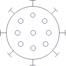
Figure 2 layout of all 26 antennas
The voltage developed in the antennas the same for a vertically or horizontally polarized incident field at 0 degrees or a field at 45 degrees or 90 degrees. However if the sphere is rotated 22.5 degrees then the field incident on one of the antennas, at the edge of the sphere, is shaded somewhat by the sphere. The same number of antennas are illuminated. However due to the change in the angle of the antennas relative to the field the reduction in induced voltage is small and in measurements at 1GHz on a prototype foil covered sphere the change in measured voltage at between 45 degrees and 22.5 degrees is only 0.483 dB and this is then approximately the isotropic deviation. This compares well to commercial probes which are specified as having +/- 1dB deviation. Rotating the antenna another 22.5 degrees places the number of antennas and their location exactly the same as in the first measurement.
The output of the antenna is connected via formable solderable semi rigid cable.
The clam shells contain three circular PCBs approximately 6.5cm in diameter.
The layout of one of the PCBs is shown in figure 3.

Figure 3 Layout of PCB
One half of the clam shell contains two PCBs and the other half the remaining PCB. The flexible formable semi rigid cables from eight antennas connect to one of the PCBs and from a further eight to the second PCB and seven to the third. The layout of the three PCBs can be identical as shown in figure 3 -The center conductor of each of the cables connect to µWave 50 Ohm resistors specified to 18GHz and the 50 Ohm is connected to a 50 Ohm microstrip etched on a μwave PCB material with a relative permittivity of 2.7. The PCB material may be either Isola IS680, Panasonic R5785 or similar. The shields of the cables are connected via a special fitting to the ground plane on the reverse of the PCB.
The microstrips connect together on the PCBs and the PCB outputs are connected together using flexible coaxial cable and then from one PCB to an SMA connector, using flexible coaxial cable, mounted at the base of one of the clam shells. So that all the antenna outputs are summed together and applied to the 1-18GHz RF detector in the base of the probes.
2. 40MHz to 1GHz probe section
This probe section is made up of one vertically oriented 10cm dipole and two horizontally oriented dipoles each connected to a differential amplifier and RF detector. Thus the outputs are dc and are summed in the summing amplifier located in the base of the probe. The amplifier converts from a differential input to single sided and from a high impedance load on the dipole, typically 1000 Ohms, to a current used for driving the RF detector shown in figure 9. Using the MOM analysis program 4NEC2D to model the dipole loaded with 1000 Ohm at 60MHz, the voltage developed in the load was -11dBm. Measuring the output of the differential amplifier, before the RF detector, it was -10dBm.
To measure the isotropic deviation in the two horizontally oriented dipole the antennas were rotated 0, 22.5, 45, 67.5 and 90 degrees with the two outputs summed. The deviation at 22.5, 67.5 and 90 degrees was 0dB, at 45degrees it was -0.9dB.
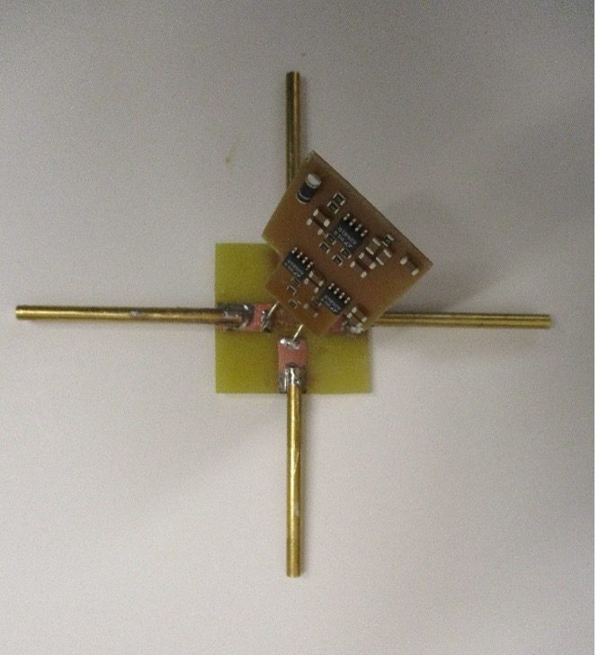
A mockup of the two horizontally oriented dipoles is shown in figure 4.
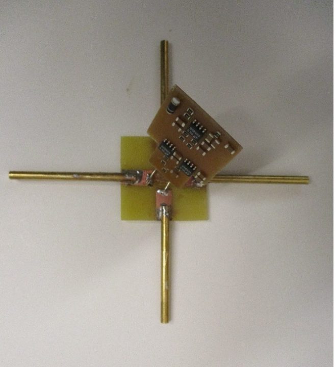
Figure 4 Mockup of the two horizontally oriented dipole with one amplifier PCB.
Only one amplifier PCB is shown whereas two amplifiers, one for horizontal the other for vertical, back to back would be required.
The differential amplifier schematic is shown in figure 5, although the RF detector is replaced by that in figure 9. A 100 Ohm resistor and 1.6pF capacitor is shown across the 1000 Ohm load presented to the antenna. This is to reduce the load impedance and therefore the voltage developed at high frequencies. Despite this the voltage developed at 1GHz and 200V/m was 6V rms which is too high for the OP Amps. Therefore some additional filtering will be required. As with the other probes the final frequency compensation should be done in the digital readout unit. The amplifier includes the 40MHz high pas filter.

Figure 5 Differential Hi Z input, filter and RF detector circuit. The RF detector is by that shown in figure 9.
The layout of the 35mm x 25mm PCB containing the amplifier and RF detector is shown in figure 6.

Figure 6 Layout of 35mm x 25mm PCB.
3. 10kHz to 40MHz probe section.
A number of designs were tried including a conductive sphere with current probes attached, a resistive sphere coated with carbon fiber and with the temperature measured by a thermistor, and a monopole with horizontal components.
Although high gain preamplifiers were used in the first two cases the designs were only effective for E fields much higher than 5V/m.
The design decided on is a non conductive 10 cm diameter sphere with 5 loops wrapped equidistant axially and vertically oriented and another 5 loops horizontally oriented. A loop starts on one side of the sphere and ends on the other side forming a circle with the ends of the vertical loops connected to the 22k Ohm load resistor and the input of the vertical amplifier. Likewise the ends of the horizontal loops are connected to a 22k Ohm load resistor and the input of the horizontal amplifier. Because the loops are made from magnet wire the enamel ensures that the horizontal and vertical loops are insulated from each other.
Figure 7 shows one horizontal and one vertical loop on the sphere

Figure 7 loops on the 10cm sphere.
The vertical loops are connected to a high input impedance differential amplifier, shown in figure 8 and the horizontal loops are connected to a second identical amplifier. The total voltage is then the sum of the output from the vertical and horizontal loops.

Figure 8 the 10kHz to 40MHz amplifier
With the vertical loops parallel to a vertical E field the loops were kept vertical but rotated in the field with no change in the induced voltage.
At the same time the induced voltage in the horizontal loops with a vertical field was monitored and these were rotated with a change of no more than 2dB.
The vertical loops were rotated relative to the field from 0 degrees to 90 degrees which means the horizontal loops were then at 0 degrees to the field.
The measured voltages from the vertical and horizontal loops were added as the loops were rotated and the measured change in the sum was no more than 2dB. Thus the isotropic deviation is close to 2dB.
The frequency response of the coils when exposed to a 5V/m field was measured from 10kHz to 40MHz.
The design goal is to have 80mV at the output for a 5V/m field and 3.52V for a 220V/m field. The design of the RF detector following the amplifier is shown in figure 9.
The amplifier shown in figure 8 contains a low pass filter at the differential input to attenuate the high frequency response. Two stages with high gain at 10kHz then followed. The 900uH inductor must be high Q and have a low dc resistance (typically 10milli Ohm). An air cored inductor would be ideal, however for 900uH the size would be a massive 40cm x 100cm. A ferrite core due to its high loss would not be a good choice. A low loss iron dust core designed for RF applications should be chosen. One with a relative permeability of 36 would result in a coil, wound with #18AWG magnet wire, of 1cm diameter and 3.6cm length. Further information on filter design and inductor design is available in reference
Only the differential amplifier with low pass filter should be located at the antenna and this was the location used during testing. The exact values of the 0.27μF and 0.28μF in the final two stages are critical and so the final design of the amplifier and filter should be made by testing.
The final correction for frequency is performed by the unit containing the single board computer outside of the test chamber.
The recommended technique for calibration of the probe and when incorporated in the final configuration with the other probes is use of a stripline antenna.
4. The RF detector
The same detector is used for the 10kHz to 40MHz amplifier and the 40MHz to 1GHz amplifier and the schematic is shown in figure 9.
The Op Amp is a unity gain amplifier with a gain bandwidth product of 1GHz. The output drive capability of the Op Amp is not high enough to drive the Schottky diode in the RF detector circuit.
For that reason a medium power RF transistor is used at the output of the OP Amp to increase the drive current. To eliminate the voltage drop, inherent in the diode RF detector, a second identical diode is used to apply a bias to the detector diode. In measurements the dc voltage across the output of the detector was 20mV with no RF applied. With the minimum 80mV generated with application of an RF field the voltage at the output is 100mV. The final gain adjustment in the digital readout corrects for the 20mV and displays 0V/m when no RF is applied.
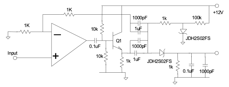
Figure 9 RF detector
5. The summing amplifier and fiber driver
The electronics contained in the base of the unit are the battery charger, battery, power supplies, summing amplifier, 1-18GHz detector, voltage controlled oscillator and fiber driver, as shown in the block diagram of figure 10.
The unit should be in a metal enclosure no higher than 4cm to ensure it fitting under a 50cm strip line antenna. No conductive cables are attached to the exterior of the unit when measuring.
The antenna cables in the non conductive tube mounted on top can penetrate through the top of the enclosure.
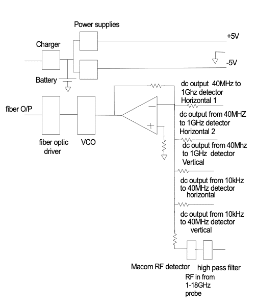
Figure 10 Block diagram of electronics in base of unit
Digital readout unit
This unit is located outside of the shielded room and is connected to the probe inside the room by a fiber optic link.
A block diagram of a possible solution is shown in figure 10. In this scheme the serial digital input from the fiber optic receiver is sent to a shift register. This is then decoded and is an input to the computer. The signal generator, used as in input to the power amplifier, is applied in the frequency ranges: 10kHz to 40MHz, 40MHz to 1GHz and 1GHz to 18GHz.
The frequency calibration of the probe over these ranges is stored in the computer and used to generate a display which show the applied field in volts/m.
The single board computer may be an Arduino.
The detailed design of this part of the probe has yet to be performed.
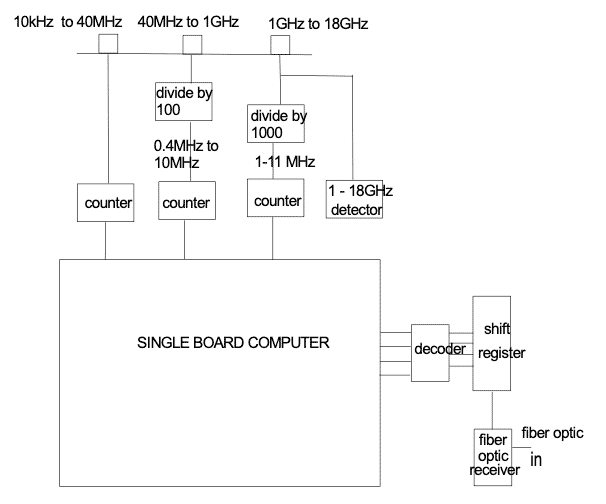
Figure 11 Block diagram of possible solution for the digital readout unit
Conclusions
One of the 1-18GHz antennas was mounted on a foil covered sphere and rotated in the field to calculate the isotropic deviation. The output was monitored at 1GHz and a field of 5V/m applied to ensure that the voltage developed was high enough for the 1-18GHz detector.
The 10kHz to 40MHz antenna was built and tested over the10kHz to 40MHz frequency range and an applied E field of 5V/m. With 5V/m applied the voltage developed at the output of the amplifier was high enough to develop a voltage at the output of the RF detector and due to the input filter should not be too high at 220V/m and 40MHz. As with the other probes the final frequency compensation is made in the digital readout unit.
The 40MHz to 1GHz dipole was built and tested over the 40MHz to 1GHz frequency range. The output from the amplifier is high enough at 5V/m but additional filtering will be required at 1GHz with an applied field of 220V/m. As with the other probes the final frequency compensation is made in the digital readout units.
Reference
- A. Weston, Electromagnetic Compatibility: Methods, Analysis, Circuits and Measurement, Third edition, 1,100 page book. 2017, CRC Press.
