Laurent Sauvage, Olivier Meynard, Sylvian Gulley and Jean-Luc Danger, Institut TELECOM, TELECOM ParisTech, Secure-IC S.A.S., Paris, France
ABSTRACT
Electromagnetic analysis (EMA) is an important class of attacks against cryptographic devices. In this article, we present two attacks to disclose the key of cryptographic implementations in FPGAs by taking advantage of EMA. The first one shows how the Correlation-based on EMA (CEMA) on a non-protected hardware AES module is possible from a distance as far as 50 cm. An analysis of the leakage structure shows that the Hamming distance model, although suitable for small distances gets more and more distorted when the antenna is displaced far from the device. We pre-characterized a physical model using a first order templates construction which allowed us to enhance the CEMA by a factor up to ten. Therefore, we conclude that EMA at large distance is feasible with our amplification strategy coupled to an innovative training phase.
The second case is about a 3DES cryptoprocessor protected with Dual-rail with Precharge Logic (DPL). We experimentally show that this countermeasure can be broken by an EMA method which relies on two stages, the first being a localisation phase by means of the chip’s cartography, and the second being the EMA attack itself on the most relevant area. We conclude that both far and near field attacks are possible: the first ones exploit the radiation of the board, while the second one the radiation of the cryptographic component.
INTRODUCTION
Nowadays the design of mathematical cryptographic algorithm is very secure and believed unbreakable, but their hardware implementation leads to a latent vulnerability against physical attacks. Physical attacks designate the analysis of the variation of different physical magnitudes during the computation of the data by a cryptographic component. An attacker is able to eavesdrop different side channels such as timing, power or electromagnetic emanation. From those measurements, she can guess cryptographic secrets thanks to statistical tools that are used as distinguishers between several hypotheses.
In 1999, Kocher et al described a side channel attack (SCA) suitable for smartcards: the power line, supplied from the card reader, was spied. Hence the name Differential Power analysis (DPA) given to this attack. With this cryptanalysis method an attacker can successfully reconstruct the secure data [1].
Two years later, Gandolfi et al introduces the principles of the EMA, ElectroMagnetic Analysis [2]. In fact Gandolfi applies the very method of the DPA to Electromagnetic emanations. EMA exploits correlation between secret data and variation in power radiation emitted. Several laboratories have worked on this topic, thus in [3], [4], Agrawal highlights that a EM probe can yield multiple EM signals via demodulation of different carriers in near and in far fields.
With the contribution of Brier et al, who introduced the CPA Correlation Power Analysis [5], Electromagnetic analysis becomes an important class of attacks against cryptographic, and more particularly Correlation-based on ElectroMagnetic Analysis (CEMA). Thanks to this cryptanalysis technique and the wealth of components in the spectrum of the Electromagnetic waves, we are now able to perform attack at distance from the chip and in near field to defeat the protection used to avoid easy attack.
In section II, we present the last results on the CEMA at distance. It is noticeable that current experimental setups allow to manage an attack at 50 cm on unprotected cryptographic components. Moreover in this section we propose a way to enhance the attack by reducing the number of measurements. Then, the section III describes the EMA applied to disclose the protection in Near Field, by cartography. Finally, section IV gives with the conclusion and the perspectives for further works.
CEMA AT DISTANCE ON A NON-PROTECTED AES HARDWARE MODULE
Correlation-based on ElectroMagnetic Analysis (CEMA) has been well studied in near-field. Some far-field experiments have been shown to be promising. However, no in-depth analysis has been carried out so far about EMA at distance. Here we introduce such kind of systematic study.
Model of Power Consumption or EM Radiation
Classically most power analysis exploit a dependence of the Hamming weight of a sensitive variable. This is referred to as the “Hamming weight model”, that consist in the number of bits in a data word set to ‘1’. But since 1998 and the introduction of CPA by Brier et al, the Hamming distance model is more widely used. It is assumed that the data leakage through the power side channel depends on the number of bits switching from one state to another one at a given time. If we consider the fact that the transition from state to state are triggered by events such as the edges of the clock signal, we can deduce that the current consumed is related to the energy required to flip the bit from one state to the next. After having introduced the model of consumption, we can now present the statistical process based on Pearson Correlation Factor for guessing the secret key.
Pearson Empirical Correlation Factor
Classical statistics introduce the Pearson correlation factor ρ(W, H) between the Hamming distance model and the measured power. It is defined as:
where W represents the measurement and H the Hamming distance. To obtain the Hamming distance model few hypotheses on the key are done. We notice that ρ(W, H) follows the Cauchy-Schwarz inequality: -1 ≤ ρ(W, H) ≤ +1. The correct key is obtained when for the right key hypothesis tends to ±1.
For further experiments we use this tool to conduct attacks.
The Test Bench
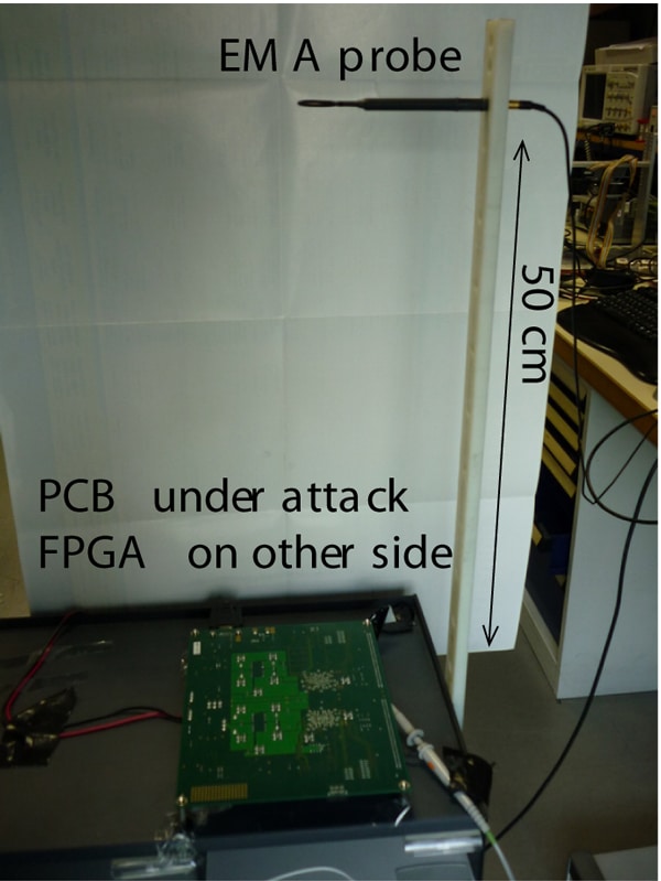
The device whose EM emanations are studied is cadenced by a clock running at 24 MHz. For these low frequencies, the usage of a Faraday cage [6] is not needed as it would induce some EM reflections and could alter the measurements. Furthermore, the size of the absorber would be too large for this range of frequencies. The material is placed on a plastic table that limits the reflection of EM radiation and avoids the conducted radiation. A plastic rod is placed perpendicularly to the board and is considered as a vertical axis to move the antenna by steps of 5 cm, as shown in Figure 1.

The targeted device is a Field Programmable Gate Array (FPGA) Virtex II by Xilinx. It embeds one AES [7] Rijndael supporting 128-bit keys. The attacked chip has no countermeasure against EMA: its implementation adheres in a straightforward manner to the NIST FIPS 197 standard. Moreover a trigger signal is outputted, each time an encryption is beginning. This saves synchronization problems. We take care of keeping far away the supply power from the chip board, in order to avoid any coupling between the radiated waves and the power supply. We record the emanations on the side with the decoupling capacitors, because the signal on this part of the board has the best quality.

The Attack at Distance on the Cryptographic Implementation of AES
First, we check that for different distances, the curves for the same plaintext are scaled down, according to an inverse power law. We notice, as expected, that the useful signal decreases following 1/di law of attenuation (where d is the distance and i a positive real number). We make the assumption that the noise reaches a limit. Indeed, the closer we get to the electronic board, the more the noise level increases, because we capture the perturbations from the board components in addition to the ambient noise. To confirm these hypotheses, we have performed an attack on the AES, when the antenna was placed much further away, at 50 cm from the FPGA board. In practice, the signal was amplified of 60 dB and averaged by a factor of 4,096. The attack needs 51,519 measurements to break the substitution box (sbox, called SubBytes in AES) #1, whereas only 1,000 are required at d = 0 cm. The correlation curve is represented in Figure 2. The correlation does not clearly stand out.
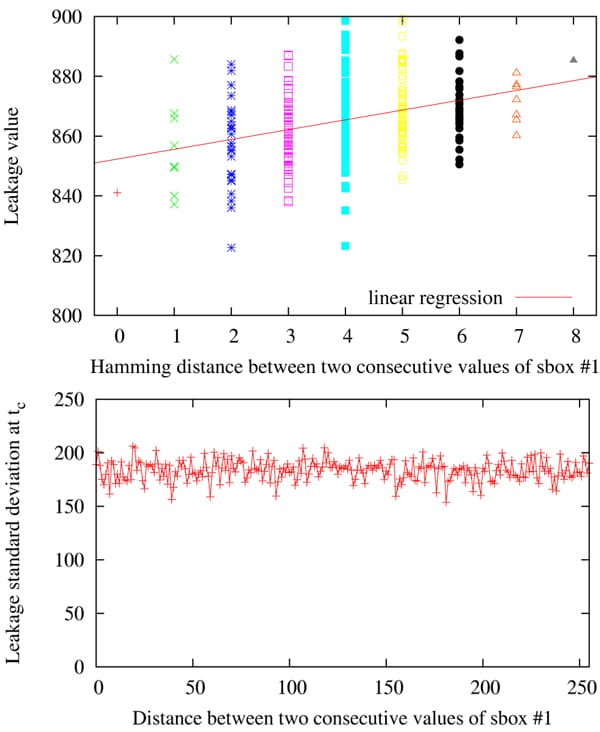
At this large distance we assume that the attack requires too many traces to fully disclose the key because the Hamming model is not holding anymore. That is why we propose a method to build an improved model based on the construction of 28 = 256 templates [8]. We indeed assume the leak of individual bit amongst the 8 that are targeted still complies with that described in II-A. Thus our approach differs from that of [9], which takes into account a dis-symmetry on the transitions edges, we will describe in Sec. III (notably in Fig. 9). However, the contribution of each bit and possible interference between them is encompassed by our template construction. We search the index tc of the maximal correlation, that corresponds to the moment when the data are stored in the register on the last round. We compute for this index the average and the variance for the 256 possible Hamming distances, the key and the message being known. This pre-characterized leakage model is shown in Figure 3.
We observe that the standard deviation is almost independent of the byte distances. Therefore, most of the model information is contained in the mean leakage value. As a consequence, we adopt a tabulated leakage model consisting in a look-up to the corresponding estimated averages. After this characterization, we launched a correlation attack on sbox #1 with the newly obtained model. The attack is considerably enhanced: the key byte entering this sbox is disclosed with as few as 5,003 traces. The correlation curve for the correct key guess is shown in Figure 4. The peak at t = tc is clearly visible, especially when contrasted with the correlation curve obtained with a classical CEMA in Figure 2.
These experiments confirm that the leakage model based on the Hamming distance model is not optimal at distance (Refer to Table 1 for attacks figures).

EMA CARTOGRAPHY ON A PROTECTED 3DES HARDWARE MODULE
In this section, we propose a method to locate any cryptographic coprocessor protected with Dual-rail with Precharge Logic. We first present the principle of this side-channel analysis countermeasure, and the cryptographic application we intend to attack. Then, we expose our localization technique, and finally give experimental results showing the gain it is able to achieve.
Dual-Rail with Precharge Logic
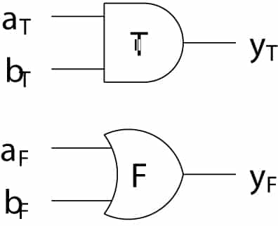
The objective of Dual-Rail with Precharge Logic (DPL) is to make constant the power consumption, and in turn the electromagnetic radiations, of an integrated circuit. Toreach this goal, each bit is represented by a couple of signals, and calculations alternate between a precharge (PRE) and an evaluation (EVA) phase. Figure 5 is an example of a DPL AND gate. In PRE, all of the inputs on the left are forced to ‘0’, which in turn forces the true output yT and the false output yF to ‘0’. Then, in EVA, after inputs toggle, only exclusively yT or yF will be set to ‘1’. This way, whatever the temporal transition, either EVA to PRE or PRE to EVA, and whatever the processed data, only one of the differential outputs commutes, yielding a constant transition count. As the power consumption is directly related to the number of transitions in CMOS technology, the activity is constant as well, whatever the variables’ values.
B. The FPGA-based Cryptographic SoPC
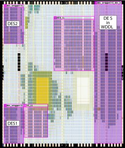
To illustrate the efficiency of our method, we apply it to a complete System on Programmable Chip (SoPC) including a master processor for I/O communication and three cryptoprocessors achieving the triple Data Encryption Standard (3DES) [10]. Although DES has been replaced by the Advanced Encryption Standard (AES) [7] since year 2001, the American National Institute of Standards and Technology (NIST) considers 3DES to be appropriate through year 2030, and the electronic payments industry still uses it for its compactness when implemented in hardware, with an area representing a quarter of AES’s. DES1 and DES2, on the top left and bottom left corners of Figure 6, are two unprotected modules which serve as reference to evaluate the security gain conveyed by the protected one. WDDL (Wave Dynamic Differential Logic [11]), the module protected by DPL, is located on the right of the SoPC floorplan. The placement is constrained by the LogicLock (LL) feature of Quartus. We have programmed this real-life application in an EP1S25 “Stratix” Altera FPGA (130-nanometer technology), embedded on a “SHIX2.0”, an 8-layer PCB (Printed Circuit Board) professional board. Note that this FPGA is not EM-shielded, thus our attack is totally non-invasive.
Spotting by Cartography
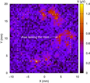
The principle of EM cartography is to measure the EM field for every point of a 2D grid covering all or only a part of the chip. This grid corresponds to the set of positions of the antenna placed by means of an X-Y motor driven table. The measurements are typically made with a spectrum analyser when working in the frequency domain, or with a digital oscilloscope in the temporal domain. Lastly, post-processing has to be applied on these measurements to obtain the final map. In the EMC area, it traditionally corresponds to extract the maximum amplitude of the EM field for each frequency component, and check it does not exceed thresholds required by standards. In the SCA topic, the post-processing has to bring out point(s) where the EM field is correlated to the cryptoprocessor activity. To locate a cryptoprocessor protected with DPL, our technique simply consists in targeting the activity of the signals controlling the alternate between the precharge and evaluation phase. In our implementation, these phases occur on the rising edge of the SoPC clock, whose frequency is 8.333 MHz. Therefore, the internal frequency of the DPL DES cryptoprocessor can be viewed as being equal to half of that of the SoPC clock, and thus equal to 4.166 MHz.The map for this latter is given in Figure 8. The dashed rectangle is a landmark which delimits the ASIC of the FPGA. On the right, the scale gives the voltage dynamic range at the output of the antenna (proportional to the EM field).
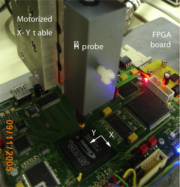
The EM field has been collected using an antenna of the “HZ-15 Probe Set” from “Rohde and Schwarz” [12], a 60 dB – 100 kHz to 3 GHz pre-amplifier, and an “54855 Infiniium Agilent” [13] oscilloscope, whose bandwidth is 6 GHz and maximal sample rate is 40 GSa/s. The antenna is mounted on a 2D motorized table and moved over the FPGA through an area of 2.08 cm x 2.00 cm. The resolution is of 50 points on X and on Y. In other words, the mechanical step equals 400 µm. Figure 7 is a photograph of the EMA experimental setup, with the antenna over the most leaking point.
In Figure 8, five areas stand out: two at the top, two at the bottom, and one large to the right of the figure. A first validation of our method is that highlighted areas are mostly on the right, which corresponds to the place of the DPL DES module in the floorplan (refer to Figure 6). The validation will be completed by analysing the results of the attack on these five points. We detail them in the following section.

EMA Attack
For all the relevant areas, new acquisitions have been launched to perform a classical CEMA. For clarity of explanation, only the best results will be presented in the rest of the paper. They have been obtained for the large area marked “Most leaking area” in Figure 8, whose center is located at X=0.416 cm and Y=1 cm. With an eye to illustrate particular phenomenons, a 256 times averaged temporal trace of the EM field at this point is depicted in Figure 9, on the left. We can observe that the EM field is positive for the precharge, negative for the evaluation. This could be explained by the current inversion of the CMOS capacitors. At the beginning of the precharge phase, the CMOS gates of DPL go from 1 to 0, whereas this is the other way round when switching from the precharge phase to the evaluation phase.
Table 2 reports the statistics for a classical Power Analysis (PA): the number of Measurements To Disclose (MTDs) the key, with the worst value grayed, the Signal over Noise Ratio (SNR) and the covariance factor at disclosure. The SNR indicator illustrates the ratio between the level obtained with the right key and those from the strongest wrong key. Results for the EMA are reported in Table 3 Its superiority to the C/DPA is well illustrated as the number of MTDs for the unprotected DES module is hundreds of times less. For DPL, CEMA able to retrieve the secret key in less than 62,976 encryptions. By considering the worst MTDs and cross-comparing them, we can conclude that the security gain of our implementation of DPL equals 7.8 against CPA, 11.6 against CEMA. It confirms that DPL brings a certain protection against EMA, yet insufficient with respect to the 5,508,224 measurements needed to disclose the key with CPA. To conclude, the proposed method is thus experimentally validated by successfully attacking a FPGA-based DPL 3DES cryptoprocessor. The accurate X-Y location of the antenna permits to gather the activity of only the targeted module, discarding the activity of others parts of the FPGA, acting as noise for an attacker.


CONCLUSION & FUTURE WORKS
This paper shows that the electromagnetic measurements represent a very efficient manner to capture the activity of a device in order to extract the secret information it conceals. We illustrate a first attack that succeeds with an antenna located at 50 cm from the targeted device. This proves that the attacker can be relatively far from the circuit by taking advantage of this non-intrusive method. The second attack is performed near the chip and allows the adversary to recover the key of a cryptoprocessor protected by DPL. Compared to DPA or CPA, the corresponding DEMA or CEMA needs much less traces. In both cases there is an evidence that the leakage is largely broadcast via the electromagnetic side channel. However some extra processing is needed to fully exploits the leaked information as it is either the sum of many electromagnetic sources (far EMA) or has to be spatially detected (near EMA). The far-field EMA exploits the global EM radiations emitted by the complete PCB, notably the power lines and the decoupling capacitors. On the contrary, the near-field EMA exploits the local EM radiations emitted by the chip’s power network.
The traces obtained from electromagnetic acquisitions have not yet revealed all their potential as there are also many parameters like the phase and frequency which could produce relevant information. Future works will then improve in a concomitant manner the processing of the traces and the attack algorithms. This implies a better knowledge of how the electromagnetic signal is generated and where are the exact sources or the best locations to consider.
REFERENCES
[1] P. C. Kocher, J. Jaffe, and B. Jun, “Differential Power Analysis,” in Proceedings of CRYPTO’99, ser. LNCS, vol. 1666. Springer-Verlag, 1999, pp. 388–397, (PDF).
[2] K. Gandolfi, C. Mourtel, and F. Olivier, “Electromagnetic Analysis: Concrete Results,” in CHES, ser. LNCS, vol. 2162. Springer, May 14-16 2001, pp. 251–261, Paris, France.
[3] D. Agrawal, B. Archambeault, J. R. Rao, and P. Rohatgi, “The EM Side–Channel(s),” in Cryptographic Hardware and Embedded Systems – CHES, ser. LNCS, B. S. Kaliski Jr., C¸ etin Kaya Koc¸, and C. Paar, Eds., vol. 2523. Springer, 2002, pp. 29–45, Redwood Shores, USA.
[4] D. Agrawal, J. R. Rao, and P. Rohatgi, “Multi-channel attacks,” in CHES, ser. LNCS, vol. 2779. Springer, 2003, pp. 2–16.
[5] E. Brier, C. Clavier, and F. Olivier, “Correlation Power Analysis with a Leakage Model,” in CHES, ser. LNCS, vol. 3156. Springer, August 11–13 2004, pp. 16–29, Cambridge, MA, USA.
[6] Y. Souissi, J.-L. Danger, S. Mekki, S. Guilley, and M. Nassar, “Techniques for electromagnetic attacks enhancement,” in DTIS (Design & Technologies of Integrated Systems), ser. IEEE. IEEE, March 23-25 2010, Hammamet, Tunisia.
[7] NIST/ITL/CSD, “Advanced Encryption Standard (AES). FIPS PUB197,” Nov 2001, http://csrc.nist.gov/publications/fips/fips197/fips-197.pdf.
[8] S. Chari, J. R. Rao, and P. Rohatgi, “Template Attacks,” in CHES, ser. LNCS, vol. 2523. Springer, August 2002, pp. 13–28, San Francisco Bay (Redwood City), USA.
[9] E. Peeters, F.-X. Standaert, and J.-J. Quisquater, “Power and electromagnetic analysis: Improved model, consequences and comparisons,” Integration, The VLSI Journal, special issue on “Embedded Cryptographic Hardware”, vol. 40, pp. 52–60, January 2007, DOI: http: //dx.doi.org/10.1016/j.vlsi.2005.12.01310.1016/j.vlsi.2005.12.013.
[10] NIST/ITL/CSD, “Data Encryption Standard. FIPS PUB 46-3,” Oct 1999, http://csrc.nist.gov/publications/fips/fips46-3/fips46-3.pdf.
[11] K. Tiri and I. Verbauwhede, “A Logic Level Design Methodology for a Secure DPA Resistant ASIC or FPGA Implementation,” in DATE’04. IEEE Computer Society, February 2004, pp. 246–251, Paris, France. DOI: 10.1109/DATE.2004.1268856.
[12] Rohde and Schwarz: http://www.rohde-schwarz.com/.
[13] Agilent Technologies:http://www.agilent.com/.
© 2010 IEEE. Reprinted, with permission, from 2010 IEEE EMC Society Symposium

