Any multi-supply pinned microcontroller can be improved simply by altering the pin allocation
Mart Coenen and Dick de Greef
Phillips Applied Technologies
Eindhoven, the Netherlands
On-chip ir drop, ground bounce, and supply bounce are key parameters that may have a serious impact on both the functional reliability and the EMC of integrated circuits (IC). This paper presents a root cause analysis of this effect, along with a separate analysis of each of these effects using a combination of integral on- and off-chip design techniques.
“IR-drop” is, according to Ohm’s Law: V= IR, where R is the equivalent path DC resistance between the source location and the device location, and I is the average current the chips draws from the supply. This DC voltage appears in between nodes of Vss and Vdd power supply distribution nets; between the boundary ground/supply pads/pins; or on any on-chip location. For each node, the summed voltage: Vir = S(DIi·DRr) from that node to the edge of the IC must be taken into account. “Ground bounce results largely from L·di/dt and occurs between the Vss pads toward the Vss plane of the PCB. In the case of “supply bounce”, a dynamic voltage variation occurs between on-chip local Vss/Vdd nets. The magnitude of supply bounce is dependent on the location considered—i.e., top metal or down at the standard cell level interconnect.
Most of the CAD tools available on the market allow for IR-drop estimation, (which in reality remains a function of time, though integrated and represented by a scalar function). The prediction of ground and supply bounce is determined by time-related functions that require substantially more data as with the IR-drop estimation.
Still, more precise information is needed. For example, a parallel bus transmitting from left to right or vice versa has no effect on the supply current drawn from the overall distribution network, but will reverse the induced voltage signature of the Vss-net/substrate voltage gradient. This “Vss-net/ substrate” effect will show up in differential vector voltage1, or in multi-pin voltage ground bounce measurements, but will have no effect on the IR-drop nor the on-chip supply bounce.
Most of the CAD tools used today, such as Mentor, Cadence, Assura, Redhawk, or Synopsis allow a pre-layout analysis of on-chip IR-drop, ground bounce, and supply bounce. The results obtained, however, will be only as good as the data used in these simulations, as analysis under every mode of operation is simply impossible. Model Order Reduction (MOR) is applied to simplify the problem down to acceptable proportions. What is not incorporated in these tools is that one can deal with the three responses mentioned by applying a combination of off- and on-chip measures.
When only the average DC (supply) current is applied to an IC, ground bounce will be reduced to zero since no di/dt is present. The non-average supply current will cause higher supply bounce fluctuations (static and dynamic) depending on the circuitry involved, its activity, and the amount of on-chip de-coupling (static versus active cells). Whether the circuit is driven by a DC voltage or current, the IR-drop remains unaffected. The IR-drop can be affected only by the number of Vss/Vdd pads used and by the amount of metal in the power distribution network. The minimum (dynamic) supply voltage occurring, at cell level, can be influenced by the circuit topology chosen—both on- and off-chip.
IR-Drop Modeling
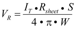
To enable modeling of multi-million transistor designs, the overall problem needs to be simplified, In actual physical designs, certain areas will draw varying supply currents over time. For the analytical analysis, the total supply current is assumed to be uniformly distributed over the IC’s supply grid. Furthermore, the equivalent sheet resistance of the Vss/Vdd net must be calculated, which is the stack-up of the various metal layers up to the top layer (Figure 1).

Depending upon the top metal structure used (possibly full metal), the sheet resistance is inversely proportional to the metal layer utilization. For example, with 20 percent metal coverage for the supply or ground grid, the equivalent sheet resistance is five times the physical sheet resistance.
VR = voltage in radial direction [V]
IT = total supply current [Amp]
Rsheet = sheet resistance [Ω2]
S = separation between the supply stripes [m]
W = width of the supply stripes [m]
A second approximation uses a circular area (with the edge at a constant voltage) to obtain an analytic expression for square or rectangular IC designs. Using this equation, the lowest IR drop can be determined, but voltage drop will appear as rotation symmetric isobars. A voltage gradient will, however, occur if the supply of the IC—i.e., the ground connections—are not uniformly distributed along this perimeter.
Dynamic Voltage Drop
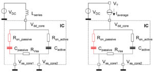
The dynamic voltage drop is a combination of several effects. The current drawn by a group of cells at a given moment is one factor. Another is the direction, or orientation, in which the supply and ground currents flow, determining the magnitude of induced voltage in the supply or ground plane. In Figure 22, the active core of an IC is supplied via an inductive connection. This supply is possible if the on-chip decoupling Cpassive is sufficiently large to sustain cycle-to-cycle operation for Cactive (typically 10 times larger). In that case, only the average supply current needs to be supplied to the core to maintain the nominal supply voltage.

When the core is supplied from a current source, the entire off-chip RF decoupling current will diminish (40 to 80 dB) as will the ground bounce resulting from L·di/dt. This reduction in ground bounce and RF supply current is very relevant for future SoC (system on chip) and SiP (system in package) architectures.
Vss-Net/Substrate Gradients
The current distribution is determined by the signal routing—i.e., the floor planning as well as the location of the decoupling cells used within that block. For example, when a clock related network is symmetrical, the induced voltage will be determined wholly by the path of integration. Nodes should be taken into consideration and may be designed such that induced voltage equals zero at the perimeter of the chip! Because the on-chip decoupling currents still flow between Cactive and Cpassive, a dynamic voltage drop will occur between the two VSS core nodes.
This model shows that placing decoupling close to the “disturbance” source will result in a reduction of voltage induced between the Vss nodes. This nodal voltage reduction is not the result of resistance induction since sheet resistance is size independent. Rather, the voltage at the boundary of the die is reduced by the resistive network in which these nodes are embedded (Figure 3).

Another issue is what will happen when the IC requires instantaneous switching—i.e., goes from idle to active mode. In this case, on-chip decoupling will be insufficient, and off-chip decoupling will be needed. Active off- and on-chip supply regulators have response time of several µs; whereas, the cycle times may be in the nanosecond, or the GHz region. Hundreds of thousands of clock cycles need to be (charge) buffered by using both on- and off-chip capacitance.
Unfortunately, when off-chip decoupling is used parallel to on-chip decoupling, the core induced disturbance currents will be divided according to the inverse ratio of impedances. When the off-chip capacitance is 100 times larger than the on-chip capacitance, 99 percent of disturbance currents will flow off-chip creating ground bounce once again.
Kelvin Contacts
In the past, methods have been developed for measuring low impedances using a four-pole measurement technique, termed a Kelvin contact. Similar techniques have also been used with large DC supply systems to measure the voltage across a load while eliminating the voltage drop across the wiring system of the supply.
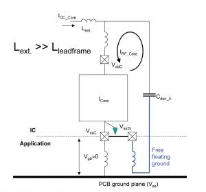
This technique is also useful for the decoupling of both on-chip and off-chip circuitry. In fact, the RF decoupling currents can be fully diverted from the average DC supply current. To achieve this diversion, extra, adjacent pads must be provided instead of a single ground and supply pad. Also, the decoupling capacitance for these extra pads must be connected to a free-floating ground that does not make direct contact with the common ground reference plane (Figure 4) of the PCB. To enhance this effect, an off-chip series inductance (Figure 2) must be applied to prevent the RF current from flowing off chip through the DC supply path. In the circuit depicted, Kelvin contacts are used only at the Vss side since a series inductance is provided at the Vdd side that is large (typically 100 times greater) as compared to the lead-frame and bond-wire inductances of the package used.

With this decoupling technique, the charge time constant increases to many µs rather than ns. Linear progressing current, rather than a RC or LC function, then represents the charging current from cycle-to-cycle. The energy (½·L·I2) is stored in the series inductance without incurring DC losses. The average supply voltage across the IC is effectively increased because the positive dip in the supply must be equal to the negative dip. Using this effect, the on-chip voltage is optimally decoupled, and a more robust design is achieved because the dynamic minimum cell voltage (excluding the IR-drop) is halved by the off-chip series inductance.
Other application areas
Kelvin contacts have been used successfully for off-chip oscillator circuitry, analog inputs, and digital off-chip parallel busses. This concept was used when severe jitter was noted in an interface between an analog oscillator block and the digital core. Using separate supply and ground pins for the digital and analog blocks, the ground bounce voltage was superimposed on the on-chip signal interface. Because the analog part was small in comparison to the digital part, the analog circuitry became grounded on-chip to the digital core.
To prevent the disturbance currents from the digital core from traveling through the analog oscillator circuitry, all off-chip connections of the oscillator were assigned as a free-floating ground. Also, the off-chip oscillator supply decoupling was connected to this free-floating ground. Ultimately, the oscillator circuitry was supplied through an off-chip series inductance (Figure 5). Applying this method reduced the oscillator jitter by more than 30 dB with only minimum design and application changes (Figure 6).


In the case of a peripheral supply, the off-chip decoupling can be assigned to an adjacent pair of VssE/VddE pins to minimize the total series impedance (loop area) of this off-chip path.
Alternatives
To reduce the off-chip noise from a digital core, a low-dropout regulator (LDO)3 can be integrated on-chip. However, the LDO causes an additional voltage drop, and it still must be followed by substantial decoupling capacitance to accommodate instantaneous change in supply currents. To this end, Kelvin contacts may be used. At the supply input pins, on-chip decoupling must be provided to build a capacitive divider with the source-drain capacitance of the power transistor used with the LDO.
Practical examples
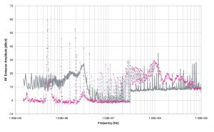
Any multi-supply-pinned microcontrollers can be improved simply by altering the pin allocation. For example, using three pairs of VssC/VddC core supply pins, a pair at minimum pitch is used as a Kelvin contact for off-chip decoupling with a free-floating ground and a series inductance. With the Vdd pins, the RF emission of the microcontroller can easily be reduced by 15 to 20 dB (Figure 7). The off-chip decoupling capacitor at the other two pairs of core supply pins must be removed before this “Kelvin contact” approach becomes effective. Similar measures can be taken for the peripheral supply of a microcontroller, DSP, etc.

Similar results can be shown for a CMOS Bluetooth SoC design when spurious emission from the RF part is suppressed by using Kelvin contacts with the baseband area (Figure 8).

Conclusions
- The use of Kelvin contacts can have a significant positive impact (20 to 80 dB) on signal integrity, power integrity, and EMC when used in the right combination—i.e., with off-chip series inductance and a free-floating ground for the off-chip decoupling capacitor.
- The application of Kelvin contacts for off-chip supply decoupling, in combination with sufficient on-chip decoupling, results in both on-chip supply bounce that is pre-determined “by design” and a reduced ground bounce.
- Kelvin contacts for decoupling create an increased margin in case of further integration towards SiP and SoC. This margin assures compatibility between sensitive analogue and RF circuitry that can be “grounded” to the common substrate or die-pad.
- The Kelvin contacts approach can be used for most existing designs that rely on multiple Vssx and Vddx pins in core, analog, and/or I/O. This approach assumes that electro-migration constraints are still being fulfilled after assigning supply pins/ balls to another “Kelvin contact” function.
- To assure an overall improvement, IR-drop and substrate/Vss-net noise must be minimized by circuit topology and floor planning. A simple analytical formula for estimation is provided. In the meanwhile, a new pre-layout IR-drop estimator has been developed which no longer requires homogeneous grids and assumes homogeneous current distributions. This paper will be presented at the EMCCompo2007 in Torino, Italy, November 28-30, 2007.
Acknowledgement
This paper is the result of work carried out under the MEDEA programme, a cooperative effort of several European semiconductor manufacturers. Specifically, this work arose from the MEDEA Mesdie (Microelectronics EMC system design for high intensity interconnect frequency environment) programme and continues under the Parachute programme. During this project, we worked closely with partners from FhG IZM, Infineon, Conti-Temic, and the University of Paderborn. Cf. the paper presented at EMC Compo, Munich, Germany, Novermber 2005.4
References
- M. Coenen, R. Derikx, “Vector voltage measurements”, Compo, Toulouse, France, November 2002.
- M. Coenen, “On-chip vs. off-chip measures, Post Academic Training (PATO), 2004
- MEDEA+ Mesdie, “Final program review”, Paderborn, the Netherlands, May, 2005.
- M. Coenen, D. de Greef, “Optimization techniques for minimizing IR-drop and supply bounce”, EMC Compo, Munich, Germany, November 2005 (Received Best Paper award.)
Mart Coenen has over 28 years experience in EMC in various fields and has published many papers and publications. He has been actively involved in international EMC standardization since 1988 and last year was awarded with the IEC 1906. He is the former project leader of the standards: IEC 61000-4-6 and IEC 610004-2 but moved his focus towards EMC in integrated circuits. At present he is convenor of IEC TC47A/WG9 and member of WG2.In addition to his career with Philips, he is co-founder of the Dutch EMC/ESD Society and part-time lecturer of Post Academic EMC courses. Aside from these activities, he owns a private EMC consulting company.
Dick de Greef studied at the ETS in Amsterdam and at the Eindhoven Technical University. From 1972 to 1979, he joined the Philips Research Laboratories in Eindhoven. Work was done in a wide field of video applications. With the Philips Consumer division, from 1979 to 1988, he was involved in the system and circuit design of ICs for video and imaging applications. In 1988 he joined Philips Semiconductors, and designed CMOS and BIMOS circuits for consumer products and image sensors for camera applications. For the same division he designed analog and digital circuits for matrix displays. In 2003 he joined the EMC group of Philips Applied Technologies, the main focus here is on EMC of integrated circuits.


