ABHISHEK RAMANUJAN, ZOUHEIR RIAH, ANNE LOUIS, Research Institute for Embedded Electronic Systems, Saint Etienne du Rouvray, France
A cutting-edge electromagnetic emission modeling tool has been presented in this paper. With most of the existing electromagnetic compatibility (EMC) analysis tools, either demanding large computational resources or being available only for expert use, this tool is principally aimed to simplify EMC analysis at the industry-level. It provides a well abstracted tooling environment for predicting and reproducing the electromagnetic radiations at component and system level. The kernel incorporates highly reliable models developed in IRSEEM. Different features and capabilities of the tool have been presented.
Introduction
Electromagnetic compatibility (EMC) has become an important consideration at the design stage of electronic components and circuits, with board or application level EMC optimizations reaching their limits. The recent European directive 2004/108/EC on EMC calls for electronic devices with very low electromagnetic emissions and high immunity to electromagnetic stress. These directives are subject to modifications in the future where the EMC constraints would definitely be tightened more than ever, making EMC one of the major causes of integrated circuit (IC) redesign. To help industries develop EMC complaint products, on one hand, the last decade has seen an indescribable growth of EMC models explaining the electromagnetic behavior of electronic components and systems, and on the other hand, the need for EMC tool development has been acute. In almost all engineering disciplines, the use and application of computer aided design (CAD) tools is widely accepted. CAD tools for EMC modeling have not kept pace with their counterparts, typically due to the large computational requirements, the need for proper understanding of all the involved electromagnetic phenomena, data confidentiality and, most importantly, their usage being limited to specialists.
Although EMC modeling tools have made the job of an EMC engineer much easier, certain problems always exist that only the expert must address. Today’s need for an EMC engineer is a dedicated modeling environment to predict and simulate the EMC behavior of electronic circuits and boards. One such tool is IC-EMC, which has been developed in an attempt to create an interface between electronic designers and vendors [1]. The tool can be used to predict and analyze the radiated emissions, conducted immunity and conducted susceptibility of integrated circuits. The modeling is based on knowledge of IBIS and ICEM data of the circuit under test, which calls for expert understanding of tool utilization. In this paper, a new industry-friendly electromagnetic emission modeling tool has been developed. It provides a front end to facilitate easy use of the generic radiated emission model developed in IRSEEM [2], [3] and enhance its productivity. The tool is well abstracted, making it a user-friendly environment and is aimed at semiconductor designers, EMC researchers and engineers.
Features
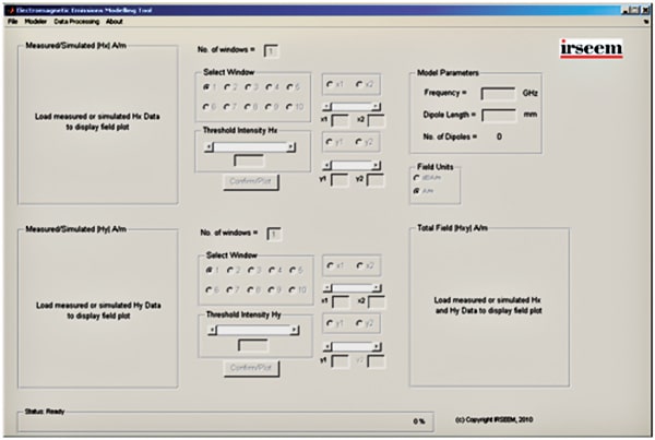
The fundamental purpose of this tool is to provide an integrated environment for modeling the electromagnetic radiations at integrated circuit and system level. The front-end is an intuitive, interactive menu-type graphical interface, making it very user-friendly. The tool incorporates two high-performing iterative frequency-domain solver technologies. These solvers are adapted for the models developed in IRSEEM as reported in [2], [3] respectively. The latter is a computationally optimized version of the former, which is capable of solving complex systems rapidly. Nevertheless, the former is also a very reliable solver for simple and small systems. After intensive tests, the kernel has been made stable for reliable usability. Depending on the selected solver type, the requisites for modeling are different. Figure 1 shows the initial screen of the tool when launched.
Figure 1. The initial screen of the developed tool.
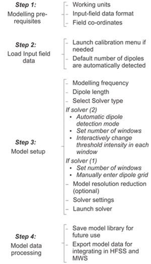
Figure 2. Modeling design flow.
The tool contains an indigenous near-field measurement calibration tool within itself, which is very practical for engineers. Raw measurement data from a spectrum analyzer (amplitude data) or a network analyzer (S¬parameters) can be converted into equivalent near-field data in a single step. The tool incorporates an interface to view the model details and the model parameters. This is intended for smart model reduction methods during post-processing of data. Once the model parameters are extracted using any one of the solvers, they can be exported for integration into industry standard commercial 3D electromagnetic tools such as Ansoft HFSS and CST Microwave Studio, as reported in [4], [5]. Additionally, the model data can be saved as a library, which can be directly imported into the tool for post-processing and future use. Figure 2 shows the design flow in order to setup a model for analysis, validation and optimizations.
Modeling Kernel
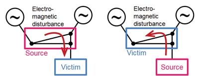
The tool implements two state-of-the-art electromagnetic emission models in the back-end [2], [3]. Depending on the chosen solver type, either of these models is used for analysis. Fundamentally, in both the models, the device under test is represented with a set of elementary electric dipoles placed on the x-y plane. The graphical representation of the models is shown in Figure 3. Each dipole in the network is represented by its position, its orientation with respect to the x-axis (θ Є R), its length (dl ЄR) and the current flowing through it (θ Є C). In both the models, the dipole parameters are extracted based on certain input details, with the use of a finely-tuned iterative optimization algorithm based on the Levenberg-Marquardt technique. The greatest advantage of the models is that they are generic, i.e. the models can be applied to calculate the radiated electromagnetic fields of any device under test, albeit, active or passive, at any height above it. No other details of the device under test are needed for modeling.
Figure 3. Geographical representation of the electromagnetic emission model.
The first model developed and reported in [2] extracts the model parameters with the dipole length and dipole positions prefixed. It takes into account the importance of the effective relative permittivity (εreff) during extraction; it therefore has to be provided as an input parameter before model extraction. Parameters are directly extracted from measured near-magnetic field measurements alone. The model has been validated on a variety of microwave devices such as microstrip lines, miniature and on-chip patch antennas, power dividers and microwave couplers. The major disadvantage of the model is the loss of computational performance when the device to-be modeled becomes large and complex. Moreover, the method is applicable only if the device possesses a unique ξreff. Nevertheless, the modeling method is highly optimized and reliable for small and simple test cases.
The second model deploys a next-generation method to extract the model parameters with the dipole length alone prefixed [3]. The method automatically detects the dipoles representing the model automatically and additionally extracts the ξreff. In this case, all the parameters are extracted from near-magnetic and near-electric field measurements. The algorithm incorporates thresholding and windowing techniques in order to detect and optimize the number of dipoles respectively. The user can interactively control the threshold intensity in each window independently. The model, as before, has been validated on a variety of microwave devices, simple and complex, as reported in [3]. The greatest advantage of this model is its capability to solve large and complex systems rapidly and efficiently.
Choosing the Right Solver Technology
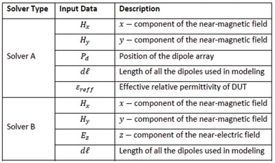
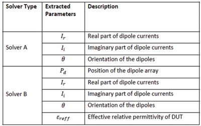
The most important step in using this tool is choosing the right solver for the right purpose. The main objective of tool development is to engineer simple solutions for complex problems. As previously stated, the tool incorporates two cutting-edge solvers, adapted for the two electromagnetic emission models presented in the previous section. The input data and the to-be extracted parameters depend on the solver selection. Table 1 and Table 2 summarize the pre-requisites and the extracted model parameters for the existing solvers. For both the solvers, the user can choose between using a dynamic Jacobian and a predetermined Jacobian. Solver A, by default, uses the finite difference method for computing the Jacobian [2] and solver B uses a predetermined system Jacobian matrix as reported in [3]. The use of solver B improves the computational time, i.e., the system is solved rapidly, with optimized memory utilization. But in a given iteration, if the Jacobian is rank deficient, solver B computes the Jacobian using the finite difference method for that iteration alone. To avoid any eventual singularity problems, the solvers compute the iteration step size using orthogonal transformations or QR decomposition technique, without compromising time and accuracy.
Table 1. Prerequisites for modeling.
Table 2. List of extracted parameters depending on the solver type.
Both the solvers have been finely tuned, intensively tested, and are extremely stable and very reliable. The only user constraint in choosing one of the solvers is when the number of dipoles for modeling exceeds 500. Though this number is just random, from various trials it is found that the use of solver A is computationally expensive and requires a lot of memory resources for more 500 dipoles. It is for this reason that the tool automatically solves the model using solver B. For smaller systems, containing 100¬200 dipoles, it is important to state that the performance of both the solvers is almost identical. In cases of using 200-500 dipoles, the user can choose between solver A and solver B depending on the availability of the input data (refer to Table 1).
Near Field Calibration Menu
The modeling environment contains an independent near-field calibration tool. It provides the right interface for an engineer if he/she intends to calibrate raw measurement data. Measurements from a network and spectrum analyzer can be directly converted into their equivalent near-field data. The calibration tool can be used for all measurements made using the international standard described in IEC 61967, part 3. Figure 4 shows the calibration menu interface.
Figure 4. Screenshot of the near-field calibration menu.
The tool consists of all the near-field measurement functionalities in IRSEEM, the probe details of standard and validated in-house probes that have been previously used and validated in several studies [2]. For certain probes, their antenna factor is built-in. For others, their antenna factor is calculated analytically. The user is also free to load a pre-calculated external file for calibration purpose. The menu can either be launched singleton or within the emission modeling environment, before loading near-field data. The user can view any component of the extracted field-data in an Excel format as shown in Figure 5. There is no restriction to the number of the viewer instances launched.
Figure 5. Data Viewer displaying the desired field component.
Setting up the First Model
A typical application of the tool is described with an example. In this case, the device under test is a complex device containing three distinct substrates as presented in [3]. The near-field simulated in Ansoft HFSS at 1 mm above the device is used to extract the model parameters and thus is loaded into the environment. Solver B, with predetermined Jacobian, is used to solve the system, which comprises of 642 dipoles. As in [3], seven windows are selected and accordingly their intensity values are chosen interactively. Figure 6 shows the modeling environment along with the loaded input details for the chosen example.
Figure 6. The modeling environment illustrated with an example.
For this test case, the model parameters are extracted in 31 iterations in a span of 11 minutes and 40 seconds on a PC with 3.2 GHz processor and 3.2 GB of RAAM. The convergence plot of the solver is shown in Figure 7. The extracted model parameters can be visualized using a dedicated “Model Viewer.” The dipole array, along with their parameters, is displayed and thus helps the user to understand the exact electromagnetic behavior of the device under test.
Figure 7. Algorithm convergence.
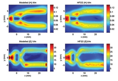
It is also possible to interactively control the current intensity factor so as to neglect the dipole sources that carry negligible current values. This is highly advantageous for model reduction and model integration into other tools. Model data can be exported from this window too. A screenshot of the “Model Viewer” window, after model extraction, is shown in Figure 8. With the model parameters extracted, it is possible to simulate and predict the electromagnetic radiations at any desired height above the device. An example of the modeled fields at a height of 22 mm above the device in comparison with those of HHFSS simulations is shown in Figure 9. It is to be noted that the HFSS simulations take about 2 hours and 37 minutes on the same PC.
Figure 8. Model Viewer interface.
Figure 9. Modeled results at 2 mm above the device in comparison with HFSS.
Conclusion
A dedicated engineer friendly EMC tool has been developed and presented in this paper. Several features and advantages of the tool have been well discussed. The tool is aimed at improving the productivity of EMC modeling methods and facilitating their application with engineers and researchers. The modeling environment consists of an independent near-field calibration tool to convert raw measurement data into their equivalent near-field. The interactive, menu-based interface provides an easy-to-use environment, without calling for expertise. There is continuous research ongoing to improve the functional capabilities of the tool.
Acknowledgement
This work was performed under the CoSiP (Chip/Package-System Co-Design) project, funded by French government via the DGCIS (Direction générale de la compétitivité de l’industrie et des services) and supported by the European commission under the MEDEA+ (Microelectronics development for European applications) program.
References
[1] E. Sicard, and A. Boyer, IC-EMC v1.5 User’s Manual, INSA editor, ISBN 978-2-87649-052-9, 320 pages.
[2] A. Ramanujan, Z. Riah, A. Louis, and B. Mazari, “Modeling the electromagnetic radiations of passive microwave components using a near-field scanning method”, IEEE Trans. Electromagn. Compat, Vol. 52, No. 4, pp. 1056-1059, Nov. 2010.
[3] A. Ramanujan, Z. Riah, A. Louis, and B. Mazari, “Computational optimizations towards an accurate and rapid electromagnetic emission modeling”, Progress In Electromagnetics Research B, Vol. 27, pp. 365-384, Jan. 2011.
[4] P. Fernandez-Lopez, A. Ramanujan, Y. Vives-Gilabert, C. Arcambal, A. Louis, and B.Mazari, “A radiated emission model compatible to a commercial electromagnetic simulation tool”, 20th International Symposium on Electromagnetic Compatibility, Zurich, Jan. 2009.
[5] P. Fernandez-Lopez, C. Arcambal, Y. Vives-Gilabert, A. Ramanujan, D. Baudry, A. Louis, and B. Mazari, “Development of a magnetic field model and insertion into a commercial electromagnetic simulator”, Turk. J. of Elec. Eng. & Comp. Sci., Vol. 17, No. 3, pp. 289-300, 2009.
Abhishek Ramanujan is currently an EMC research engineer working in the Research Institute for Embedded Systems (IRSEEM). He received his Electronic and Telecommunication Engineering degree from Vellore Institute of Technology, India in 2007, the Masters Research degree in microelectronics from the University of Rouen, France in 2008 and a Ph.D degree in Electromagnetic Compatibility from the University of Rouen in June 2011. His research interests include electromagnetic compatibility modeling, embedded systems, and microelectronics.
Zouheir Riah received his electronic engineering diploma from the University of Constantine, Algeria, in 1996, and Masters Research degree in Optoelectronic, optics and microwave from the Grenoble Institute of Technology (INPG) in 2001. He obtained his Ph.D degree in Non-Linear Circuits and Sub-systems in February 2005 at the University of Limoges and completed his post doctoral fellowship at the Research Institute for Embedded Systems (IRSEEM), Rouen, France in 2008. He is currently a lecturer-researcher at ESIGELEC (Graduate Engineering School) – IRSEEM. His research interests are about near-field active probes.
Anne Louis received her M.Sc degree in Electronics, Electrotechnics and Automatics from the University of Limoges, France, in 1994. In 1995, she joined the XLIM research institute (formerly IRCOM) where she was involved in broadband active filters design methods. She received her Ph.D in Microwave communications from IRCOM, University of Limoges, France in 1998. In 1999, she joined ESIGELEC, Graduate Engineering School, Rouen, France, where she is currently a lecturer in electromagnetism and microwaves. Since 2003, she is the Head of the Electronics and Systems department of the Research Institute for Embedded Systems (IRSEEM). In 2006, she was entitled to supervise research (HDR) and she is the Director of Doctoral Training at ESIGELEC since 2008.

