It is fairly common to find multiple onboard DC-DC converters on today’s portable, mobile, and IoT devices. If the device uses wireless, GPS, or cellular technologies, the EMI from these converters (which generally use switching frequencies between 1 and 3 MHz) often interferes with the receiver performance of the wireless modules.
The problem really crops up for low-band cellular (700-900 MHz) or GPS (1575.42), and perhaps less so for Wi-Fi (2.4 GHz), as the harmonic emissions from these converters often extend up to 2 GHz, or more. Cellular providers have strict receiver sensitivity requirements and Total Isotropic Sensitivity (TIS) is one of the tests performed during CTIA compliance. If the receiver is not sensitive enough, the product will not be allowed onto the cellular system (References 1 and 2).
This article describes the top ten methods for reducing the emissions from these DC-DC converters. They are listed in no particular order – ALL are important.
1. Specify low-EMI converters. Both Texas Instruments (TI) and Analog Devices / Linear Technologies (AD) continue to develop low-EMI devices. AD recently developed their Silent Switcher, which accommodates locating the input and output capacitors particularly close to the IC package. Their newer Silent Switcher 2 low-EMI converters incorporate both the input and output capacitors and their associated loops, within the IC package. Finally, their “µModule” series of converters also incorporate the output inductor, as well. While more expensive, these are all particularly quiet for EMI.
2. Use a proper PC board stack-up. Most of my clients get this wrong (Figure 1). All signal layers must have an adjacent ground reference plane (GRP) and all power traces (or planes) must also have an adjacent GRP (Figure 2). This is because all microstrip, stripline, and power routing should be considered transmission lines in today’s fast digital technol- If this rule is not followed, expect noise and signal coupling between circuits (one form of crosstalk), radiated EMI, and board edge radiation directly into the antenna.
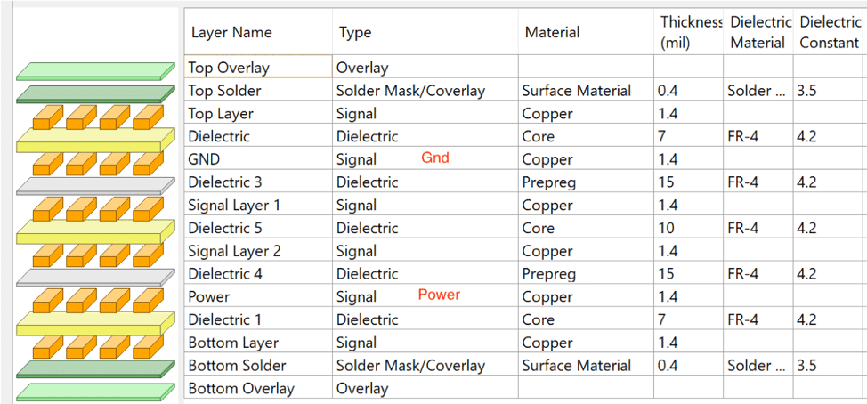
Figure 1 – A very common, but poor, EMI stack-up design (6-layer example). Signal layers 4 and 6 are referenced to power, while the GRP and power planes are non-adjacent with two signal layers in between. This will couple power transients on those two signal layers.
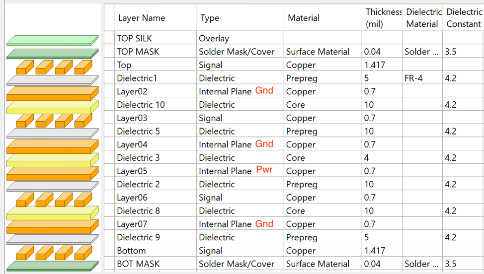
Figure 2 – A good EMI stack-up design (8-layer example). All signal layers are referenced to an adjacent GRP, while power is also referenced to an adjacent GRP.
3. The ground reference plane (or planes) must be solid. Fast switching signals or converter traces crossing gaps or slots within the ground reference plane (GRP) will couple EMI throughout the board and can couple into sensitive Note that some of TI’s older data sheets (Note 1) recommend carving away the GRP (and all other signals) from around the path of the circuit trace from the converter SW node to the input of the output inductor. This is incorrect! This trace MUST be adjacent to a solid GRP. Otherwise, their layout suggestions are OK. Please refer to the video demo explaining why gaps in the GRP are a disaster for EMI (Reference 3).
4. Keep all DC-DC converter circuitry on the top layer and over an adjacent GRP. One issue that creates noise coupling is running fast switching signals from the top to bottom of the PC board. I had one client locate the converter circuitry on top and the output inductor at the bottom of their board. The resulting 3 MHz switching currents flowing from top to bottom and back created enough interference to block onboard GPS reception. If fast rise-time signals must be routed from top to bottom, this generally requires an adjacent stitching capacitor (connected power to GRP) located next to the via to provide a nearby return path for the signal current back to the source.
5. Keep all DC-DC converter circuitry extremely close to the converter IC. DC-DC converters always have an input current loop and an output current loop (Figure 3). These loop areas must be minimized! IC manufacturers are starting to recognize EMI is an issue and warn designers about The converter manufacturers often (towards the end of the data sheet!) offer a suggested layout. Layout suggestions in the last 2-3 years are usually accurate. If older than that, are often incorrect. Both the input and output capacitors, along with the output inductor, should be located as close to the IC package as possible to minimize these loops.
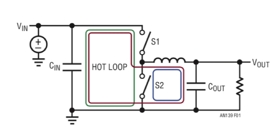
Figure 3 – An illustration showing the two “hot” current loops in typical DC-DC buck converters; one on the primary input and one on the secondary output. Courtesy, Analog Devices / Linear Technology AN-130.
6. Locate DC-DC converter circuitry close to the power entry of the board. This will tend to localize the switching currents away from sensitive wireless modules (Reference 4). However, there may be cases where the wireless module manufacturer wants a converter located near the module. If this is the case, observe all the other rules and face an increased risk in EMI coupling directly to the antenna!
7. The output inductor should be a shielded design. There are two types of inductor; shielded and unshielded. Always use a shielded inductor, because this tends to confine the magnetic H-field If you can see the windings, it’s an unshielded design!
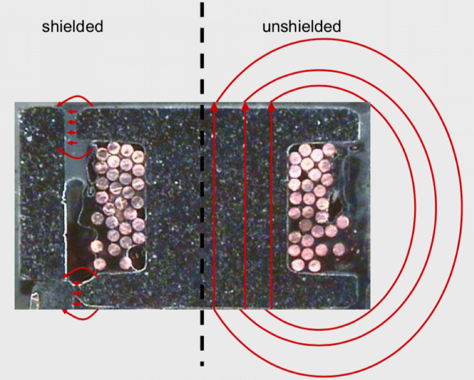
Figure 4 – A cross-section of two typical ferrite core inductors. You can see the turns in the unshielded style (right side), but not in the shielded style (left side). The extra ferrite shield confines the magnetic field much better (red arrows). Courtesy, Würth Elektronik eiSos.
8. Orient the output inductor for the lowest EMI. Inductors have a “start” and an “end” on the winding. The start terminal is sometimes marked on the top of the body with a half-circle or dot. Because the start of the winding is buried by the total turns, it is somewhat shielded by those same turns. Orient the start of the winding so it connects to the switched output (often labeled “SW”) of the DC-DC converter IC. The end of the winding connects to the output filter, so it’s going to be quieter than the start of the winding.
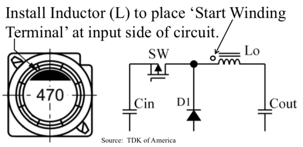
Figure 5 – Some ferrite inductors have a mark of some kind, such as TDK’s half-moon, indicating pin 1 (the start of the winding). On Würth Elektronik parts, this is generally a dot. Courtesy Rick Hartley Enterprises and TDK of America.
9. The DC-DC converters will likely require local shields. Despite the use of magnetically-shielded inductors, good PC board design, and layout practices, there will still be a strong H-, and especially E-fields, generated around the circuit loops and output Design your PC boards to accommodate these local shields at the start by adding “fencing solder strips” connected to the GRP. If you don’t need them, great.
10. Locate antennas and coax cables far from converter circuitry. Antennas and their associated coax cables, if used) should be located as far as possible from DC-DC The input circuit loop of large voltage drop buck converters will have a relatively high dV/dt and the associated electric field can couple directly into the receiver.
______________________________
Note 1 – Some of TI’s older data sheets (examples below) recommend removing the GRP surrounding the output node (and sometimes the input node, as well) of their DC-DC converter designs or demo boards. This is incorrect, in my opinion, as noted above in Tip 4.
- SLVU437A (rev 7/2013) – TPS621X0-505 EVM series
- SLVSAG7E (rev 8/2016) – TPS62130-series
- SLVC394 – Gerbers for the TPS62130-series demo board
REFERENCES
- Wyatt, Platform Interference – Measurement and Mitigation, Interference Technology, https://interferencetechnology.com/ platform-interference-measurement-mitigation/
- Wyatt and Sandler, Top Three EMI and Power Integrity Problems with On-Board DC-DC Converters and LDO Regulators, Interference Technology, https://interferencetechnology. com/top-three-emi-power-integrity-problems-board-dc-dc- converters-ldo-regulators/
- Fast clock trace over gap in return plane (video), https://www.com/watch?v=L44lTnQgv-o&t=9s
- André and Wyatt, EMI Troubleshooting Cookbook for Product Designers, SciTech Publishers.


