A technology roadmap is a tool for attaining the optimum development within a sector of technology.
Marcel van Doorn
Philips Electromagnetics & Cooling Competence Center, Eindhoven, the Netherlands
INTRODUCTION
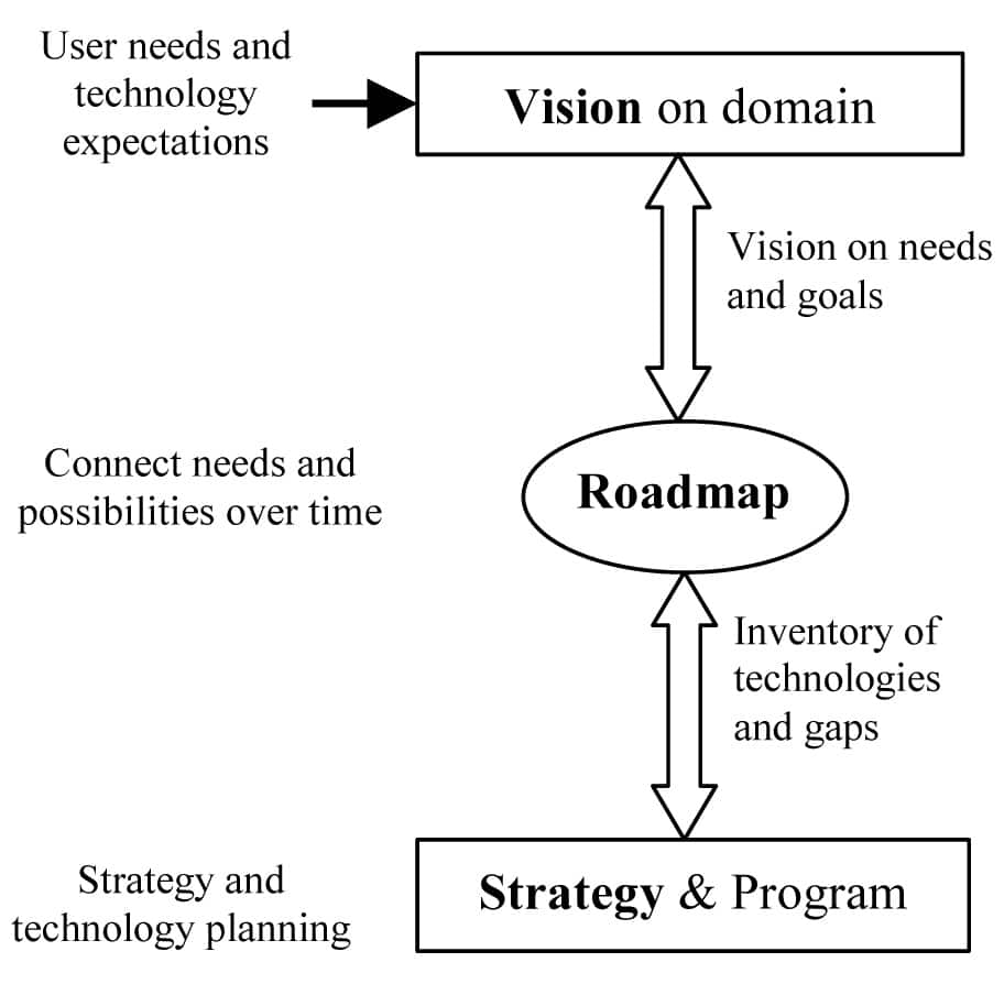
This article expands earlier work on the concept of a technology roadmap for EMC technology.1 Just as a traditional terrestrial map helps insure that travelers arrive at their destination safely, a technology roadmap is a tool for attaining the optimum development within a sector of technology. Like all maps, an overarching perspective allows a view of the overall terrain including valuable resources and possible obstacles.
The process for obtaining a technology roadmap for a specific domain calls into play both vision development and strategy definition. Figure 1 depicts the technology road-mapping process.2, 3 A typical time span for a technology roadmap is five to ten years, although for certain technology domains, 50 years or longer is not inconceivable (e.g., energy and space technology).
In this paper the road-mapping process will be applied to the domain of EMC technology. The particular characteristics of this domain are described, and future technological developments necessitated by evolving developments in the electronics industry are listed. Also included are the framework for an EMC technology roadmap and some examples of EMC technology needs and possibilities projected over a given time span. Based on the EMC technology gaps, a long-term EMC research program can be defined and planned.
THE EMC TECHNOLOGY DOMAIN
Precisely, what is the EMC technology domain? Whenever an electronic device is adversely affected by an external noise source, electromagnetic interference (EMI) is present. If an EMI problem exists, there is always a disturbance source, a victim (susceptible device), and a coupling path. Figure 2 illustrates this troubling “triptych” along with some of the examples of noisy and susceptible devices.
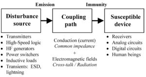
Practitioners of electromagnetic compatibility (EMC) strive to change culprit and victim into two devices that can operate harmoniously in the same vicinity. The frequency range of interest extends from DC to 400 GHz. Interference can be reduced by altering the source, victim, or coupling path. Some typical interference reduction techniques include: spacing, filtering, decoupling, isolating, shielding, grounding, and circuit design. These techniques can be employed at component, printed circuit board (PCB), cable and connector, cabinet, or system level.

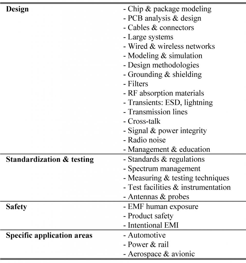
An international regulatory framework has been established to control emissions and to ensure that equipment is immune to EMI. Failure to comply with EMC constitutes a product liability risk and bars access to the marketplace. Table 1 is an overview of vital topics within the EMC domain. These subjects have been presented at international EMC conferences over the last 15 years. The various subjects have been classified into four main categories: design, standardization and testing, safety, and specific application areas. Using this overview, a general breakdown on EMC and electronic systems is possible (Figure 3). Application areas range from consumer electronics to crucial military systems. Each application consists of the main building blocks: components, interconnects (wired or wireless), subsystems, and the completed system. In some applications, different systems work together in a network. The significant EMC issues in all these applications can be reduced to three main challenges—design, standardization, and safety. Clearly, the trends and needs within these three areas of technology must be carefully examined.
TRENDS AND NEEDS
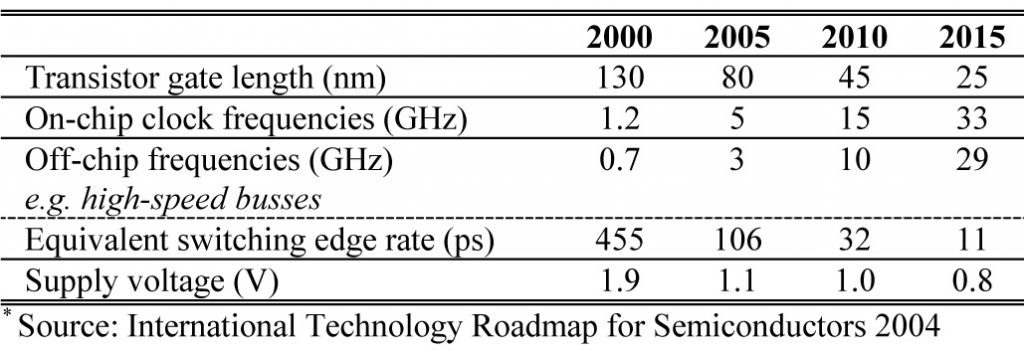
The main building blocks of an electronic system are the integrated circuits (ICs). According to the International Technology Roadmap for Semiconductors,4 the communication speed between the chips is increasing and is projected to be 10 GHz with an on-chip clock of 15 GHz in the year 2010 (Table 2). Given this projection, logic thresholds will be lower, the noise margin will decrease, and ICs will become more vulnerable to interference. Radiated emissions will increase because of faster switching edges and the concomitant increase in energy in an harmonic spectrum that extends to higher frequencies. Over the coming decade, the number and variety of potential disturbance sources and victims is set to increase exponentially—leading to an astronomical increase in the risk of interference. Consequently, controlling this interference is becoming a key issue in system design.
The market needs safe, secure, highly reliable, low-cost products that are interference-free and EMC-compliant. To achieve this goal, new methods and tools must be developed to reduce emissions and to boost the immunity of components, interconnects, and subsystems. The future electromagnetic environment must be controlled by legislation and standardization with new test methods, frequency bands, and limits.
EMC Design
A high-speed digital lifestyle (including digital radio/TV, Internet, and new applications and services) is fast emerging. By 2010 all products will incorporate digital technology. Multimedia products combine radio, TV, PC, and wireless functions. Such device integration only increases the risk of self-pollution. The explosive growth in the popularity of wireless devices will lead to greater interference challenges. In-home digital wired and wireless networks will cause non-traditional EMI scenarios.
Time-to-market and product life cycles are becoming increasingly shorter. For consumer electronics, the first six months on the market are the most profitable. If the product launch is delayed, a significant share of the life-cycle profits may be lost. EMI problems can thwart speedy movement along the critical path of product creation. The risk of re-design must be reduced, and design efficiency must be improved. Better design methodologies are needed to reduce emissions and to increase immunity. Possibilities include simulation/diagnostic tools, new design rules, and expert systems in CAD tools.
An integral EMC design approach is needed to achieve an optimum cost-effective integration of technologies at the chip, package, board, cable, module, enclosure, and system level. Signal integrity (SI) thermal, software, and cost must be factored into any effective approach.
EMC Standardization
Overall trends and needs in the area of EMC regulation have been identified.5 Crucial areas for improvement include:
- More and stricter EMC regulations must be developed for products with high clock frequencies, for digital modulation techniques, and for wired and wireless communication devices. An increase in the number of microprocessors in homes, businesses, factories, and vehicles will lead to a rise in interference problems. New emission and immunity test methods must be developed for higher frequencies (mode-stirred chambers, fully anechoic rooms, etc.)
- Reassessment of present EMI limits is warranted given the changes taking place in the electrical environment. EMC practitioners must develop a database of defined protection levels for radio services that can be used as a basis for deriving future EMC limits.
- Developing test methods for digital services is needed because current EMC test methods have their origins in analog technology, and limits are based on the protection of analog radio and TV services below 1 GHz. Digital radio services have tolerances to broadband and narrowband interference that differ from those of analog services. There is an urgent need to investigate the impact of these differences when determining interference limits and test methods for digital radio/TV products. Resolving the digital EMC problem will be a major challenge in the coming decade.
- Technology convergence is clearly evident in multimedia products (e.g., TV and PC). At the present time, such multimedia products must be tested for compliance to several standards (CISPR 13 and CISPR 20 for TV, CISPR 22 and CISPR 24 for the PC). There is an urgent need to address this unreasonable cost burden in EMC standardization.
- The EMC of networks and installations constitute the “missing link” in the current mass of EMC standards. Many wired home networks use existing power or telephone wiring and—without coordination—such an arrangement will lead to EMC problems.
EM Safety
EM fields and health are matters of growing concern regarding the potentially harmful effects on human beings of exposure to electromagnetic fields (EMF). Standardization bodies in Europe, and worldwide, are developing standards to limit EMF exposure for humans. The goal is to prevent any known adverse effects on health caused by exposure to electromagnetic fields in the frequency range from 0 Hz to 300 GHz. Legislation requires compliance with EMF standards. To comply with the new EMF standards, new EMF competence must be developed. “EMF safety” must be integrated into the product creation process—from specification to design, qualification, and production. New testing, simulation, and assessment tools that determine product and work environment compliance with EMF standards are needed. At the same time, new EMF design and application/operation guidelines must be developed. Future expansion of wireless connectivity, wearable electronics, and innovations in healthcare compound the need for careful investigation of EMF issues.
Product safety issues must be addressed. All electronic devices are subject to errors or malfunctions caused by electromagnetic interference. A functional safety perspective on EMC is needed in those cases in which errors could result in injury or harm to the health of users. Failure to do so puts consumers in jeopardy and leaves manufacturers exposed to financial risks including liability lawsuits, product recalls, negative publicity, and loss of consumer confidence. In fact, the risks caused by EMI-related functional safety lapses are increasing because of:
- Rapidly increasing use of electronics in safety-related applications,
- Worsening electromagnetic environment,
- Increasing use of electronic devices.
- At the present time, neither safety nor EMC standards adequately control EMI-related functional safety issues.6
Intentional electromagnetic interference (IEMI) refers to the deliberate attempt to produce electromagnetic radiated and conducted disturbances that interfere with the operation of equipment. Such an act could be carried out for criminal purposes. The thrust of present research is to determine the feasibility of such attacks, to determine ways to detect such attacks, and/or to prevent the disturbances that might be generated. Clearly, methods must be developed to protect equipment and systems from electromagnetic disturbances (e.g., high-level transients) of a hostile origin.
THE EMC TECHNOLOGY ROADMAP
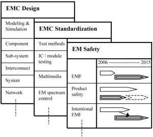
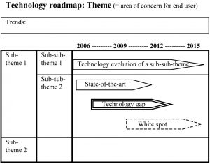
Figure 4 shows a template that could be used to create a technology roadmap. The title specifies goals for the technology sector under scrutiny. The upper frame shows the trends within this sector. Preferably, quantitative figures should be used within this trend frame. The first two columns indicate sub-themes or areas of technology that pose challenges if the goals embodied in the title are to be realized. The third column depicts the evolution of a sub-theme over time. The arrows can be coded in a single, double, or dash-lined style. A single-line arrow represents state-of-the-art technology that still needs research development and assessment. The double-line arrow represents a technology gap that requires the development of competence and capacity if crucial timely development is to take place. The dashed-line arrow indicates a white spot, i.e., a technological challenge for which there is no clear solution at present. It is important to emphasize that the technology roadmap is not a project plan, but a map showing the evolution of technologies over time. Detailed planning of project activities for achieving new technologies is part of the strategic research program.
This analytical approach could be applied to the main aspects of the EMC technology domain: EMC design, standardization, and safety. A roadmap for each of these areas encompasses the complete EMC technology domain. Figure 5 shows an EMC technology roadmap framework based on this approach and indicates some important sub-themes. Interactive workshops and consultation with experts in the fields allows the “cartographer” to develop a more detailed map and to fill in crucial details.
Working with one sub-topic “Modeling and Simulation” is illustrative of the overall process (Table 3). Sub-topics within EMC standardization, “Multimedia” and “IC/Module Testing” are detailed as well (Table 4). The roadmaps in Tables 3 and 4 cover the time span of 2006 to 2015.


Modeling and Simulation
In Table 3 some trends in the field of EMC design are indicated. Clearly, frequencies have increased from the MHz to the GHz domain, a development corresponding with the change in wavelength from meters to centimeters. This distinct change explains why, in the past cables attached to boards and systems were the likely suspects for causing radiated emissions. In the future, tracks on the PCB or even the IC packages will be tagged as likely interference sources.
Design tools that simulate the signal integrity behavior of ICs and PCBs are already quite mature. Unfortunately, a complete EMC analysis at IC, board, or system level is still not possible. Correct modeling is an extremely important, but also very complex, part of this analysis process. Fast computing electromagnetic algorithms are needed to make analysis tools user-friendly. Synthesis tools that can define the optimum EMC architecture of a complex system do not exist as yet—a crucial “white spot.”
Eventually, EMC expert systems will close the gap between subsystem and complete-system simulations. Modeling and simulation within well-defined problem areas should bring new insights and design guidelines at IC, board, and system levels. These discoveries will be integrated into more comprehensive expert systems and design tools.
Multimedia
The current emission and immunity standards for Audio/Video (CISPR 13 and 20) and Information Technology Equipment (CISPR 22 and 24) will merge into a new product standard for Multimedia equipment (CISPR 32 and 35). To guarantee satisfactory protection of digital radio receivers of wireless communication systems, a new weighting factor should be developed with a new limit. For immunity testing, a Unified Disturbance Source should be developed representing the typical disturbance characteristics of the most commonly used digitally modulated communication signals. These are clear examples of technology gaps in the field of multimedia EMC standardization that should be addressed.
IC/Module Testing
Recently, measuring methods to characterize the emission and immunity behavior of integrated circuits in the frequency range 150 kHz to 1 GHz have been defined (IEC 61967 and IEC 62132). In the coming years, experience in creating actual designs using these state-of-the-art test methods should bring further refinements. Correlations between the different test methods should be investigated. Technology gaps in the field of IC testing are found in the standardized emission and immunity test methods above 1 GHz. There is an urgent need for the semiconductor industry to develop such test methods. Also, the correlation of EMC requirements at the system level to EMC limits at the IC/module level is an important area of investigation worthy of more attention.
An EMC technology roadmap identifies both the critical enabling EMC technologies needed by future markets and the technology gaps between existing technologies and those that will be required. It helps to define a strategic long-term research program needed to speed up the introduction of new technologies in our society. The document resulting from the EMC technology Road-mapping process is a first step towards technological innovation. After creating the roadmap, the plan must be implemented. Research and development are expensive, and reduced budgets are making it impossible for individual companies to pursue independent development of all the technologies they might need to meet future market requirements. Collaboration and partnerships between companies and universities should be encouraged to help realize needed EMC research and development goals.
CONCLUSION
The technology road-mapping process is an efficient tool for identifying, selecting, and developing EMC technologies that will satisfy future market needs. This paper represents an initial step towards defining a framework for an EMC technology roadmap. The most important EMC technology topics were explored under the categories of EMC design, standardization, and safety. Technology roadmaps relating to EMC design and standardization provide examples of the process.
Teams of experts from major industries and research institutes must develop a roadmap that will identify emerging market requirements and challenging EMC technology gaps. This roadmap will help to determine the strategic research choices that companies and policy-makers must make. This unified effort will integrate EMC technologies successfully in tomorrow’s world creating an electromagnetic-friendly and secure society.
NOTES
The European Technology Network on Sustainable Electromagnetic Environments has used the presented roadmapping process, which has resulted in the brochure “Vision 2020:The EMC Technology Roadmap.” The brochure may be downloaded at www.emc-esd.nl (link:ETN-SEE).
REFERENCES
1. M.J.C.M. van Doorn, “EMC Technology Roadmapping: A Long-Term Strategy,” Proceedings of the 17th Zurich International Symposium on EMC, Singapore, 2006.
2. L. Eggermont, a.o., “Embedded Systems Roadmap 2002,” STW Technology Foundation/PROGRESS, ISBN: 90-73461-30-8, March 2002.
3. “MEDEA+ Applications Technology Roadmap,” MEDEA+ office, Version 1.0, Nov. 2003. http://www.medea.org/.
4. “International Technology Roadmap for Semiconductors 2004”, http://public.itrs.net/.
5. P. Kerry, “EMC Standards – Quo Vadis,” IEEE EMC Istanbul, 2003.
6. K. Armstrong, “EMC for Functional Safety,” IEEE Symposium on Product Safety Engineering, Santa Clara, CA, 2004.
Marcel van Doorn was born in Tilburg, The Netherlands, in 1954. He received the B.Sc. degree in electrical engineering from the Technical High School of Eindhoven, The Netherlands in 1976, and the M.Sc. degree in electrical engineering from the University of Eindhoven, the Netherlands in 1981. From 1982 to 1986 he worked at the Dutch Railways in Utrecht on the electromagnetic modeling and simulation of train detection systems. In 1986 he joined Philips Consumer Electronics, where he has worked in many different areas of the electromagnetic compatibility (EMC) domain, from testing and standardization, to consultancy and research. He has presented many international EMC training sessions within Philips and to post-academic students. Currently, he is the Technology & Strategy Manager of the Philips Electromagnetics & Cooling Competence Center and responsible for the EMC technology roadmap for the coming years.


