Transmission lines, antennas, and RF measurement systems all rely on a single electromagnetic model – the plane wave solution to Maxwell’s equations.
While often treated as a theoretical result, this solution governs how energy propagates, reflects, radiates, and ultimately contributes to interference in real RF hardware.
There are several, heavy hitting RF applications that are reliant on plane-wave-based models.
General RF Design Parameters
When designing RF circuits, there are 8 parameters that govern how electromagnetic energy propagates through a structure – phase velocity, wavelength, wave impedance, phase constant/wave number, attenuation constant, propagation constant, skin depth, and surface resistivity.
These are not independent variables. They are directly derived from the forward and reverse plane-wave general solution to the 1-D Helmholtz equation:
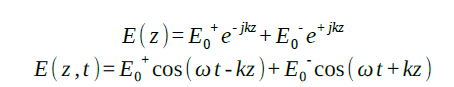
The propagation constant, γ, combines the effects of phase shift, β, and attenuation, α:
γ=α+j β
The phase constant/wave number, β, describes how both amplitude and phase evolve as a wave travels through a medium. The phase constant sets wavelength/electrical length:
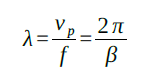
At RF/Microwave frequencies, geometry is measured in wavelengths. Trace length, resonator sizes, and antenna dimensions are all governed by this exact relationship.
The attenuation constant, α, describes exponential decay of the wave as it propagates. It captures conductor and dielectric losses and directly determines insertion loss in practical structures.
Wave impedance, η, arises from the electric-to-magnetic field ratio in the plane-wave solution:
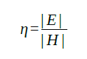
This electric to magnetic field relationship underpins characteristic impedance in transmission lines.
A 50 Ohm transmission line is simply a geometry engineered to enforce a specific plane-wave electric to magnetic field ratio.
Without this controlled electric to magnetic field ratio, it would be impossible to even begin engineering impedance matching networks, because the characteristic impedance of the medium would be uncontrollable.
In conductive media, the lossy plane-wave solution yields skin depth and surface resistivity which determines RF/Microwave conductive losses.
Skin depth in particular is crucial in determining how thick to make microstrip/stripline traces as higher frequency signals only penetrate through a thin layer of the conductive media.
Taken together, all of these parameters are not standalone formulas, but direct consequences of Maxwell’s equations expressed through the plane wave solution.
In practical RF systems, misunderstanding these parameters will lead to performance degradation and interference.
If the propagation constant is not properly accounted for, electrical lengths shift, resonances move, and unintended radiation peaks can appear.
If attenuation is underestimated, insertion loss increases and available system power decreases. If the characteristic impedance is poorly controlled, reflections increase and will raise the probability of unwanted radiation.
All of these variables are not abstract. All 8 parameters determine whether an RF design operates efficiently or becomes a source of interference.
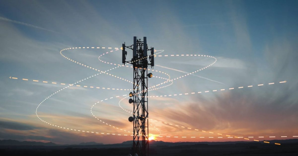
Far Field Antenna Characteristics
For antenna’s, the far field of an antenna is where the radiated fields locally resemble a plane wave.
Close to an antenna, the fields are complex, spherical, and still evolving – great for applications such as RFID and near-field communication, but not effective for cellular systems, SATCOM, WiFi, broadcast radio/television, and radar systems – all of which rely on plane-wave behavior.
In terms of design, antenna gain and radiation patterns are defined in the far field. Only in the far field, the angular field distribution becomes distance-independent, the electric to magnetic field ratio stabilizes, and the Poynting vector represents real outward power flow.
This allows engineers to measure radiation patterns, beamwidth, and directivity.
In practical terms, this far-field plane-wave behavior is what allows regulatory radiated emissions measurements to be meaningful. Compliance limits assume far-field conditions where the field strength scales predictably with distance.
If a system unintentionally radiates, the resulting emissions behave according to this same plane-wave model. In other words, the same physics that enables long-distance communication also governs how interference propagates away from a device.
Anechoic Chambers
An anechoic chamber is designed to simulate free space by lining the walls with RF absorbent material to minimize reflection with a fixed/controlled antenna acting as the field source.
This is typically done to measure another antenna or emissions related device. The RF absorbent material on the walls of the chamber attenuate incident waves from the source antenna so reflections are drastically reduced and ensures that the dominant field at the measured device behaves like a propagating plane wave.
Maxwell’s plane wave solution assumes an infinite homogeneous medium with no reflections or boundaries. In a normal room, these assumptions collapse. Waves reflect off walls, standing waves form, and the electric to magnetic field ratio becomes unbalanced.
The anechoic chamber exists to restore plane-wave conditions/free-space physics. For radiated EMC or antenna testing, we typically want one dominant forward propagating wave, little reflection, a stable wave impedance, and predictable power density spreading.
Anechoic chambers and EMC testing in these chambers provides these necessary conditions by simulating free-space plane wave behavior.
If plane-wave conditions are not approximated, measurement uncertainty increases dramatically. Reflections create standing-wave patterns, causing spatial field variations that can artificially inflate or suppress measured emissions.
This is why absorber performance, chamber geometry, and antenna placement are tightly controlled in EMC testing. The chamber is not simply a quiet room – it is an engineered attempt to restore the assumptions of the plane-wave solution.
Enjoying this article?
Subscribe to Interference Technology for expert coverage of EMI, EMC, and signal integrity challenges—plus immediate access to new digital magazine issues.
Subscribe here →
RF Measurement Systems
Modern RF measurement systems are fundamentally rooted in Maxwell’s wave solutions. Even though these instruments measure quantities such as voltage and power, the underlying physics governing these measurements is electromagnetic wave propagation.
Instead of waves spreading in free space, the fields are confined between conductors, forming guided electromagnetic modes determined by boundary conditions.
For example, consider a coaxial cable connected to a VNA. The signals are not purely voltage and current in a circuit-theory sense, but guided electromagnetic fields propagating between two conductors.
At the core, these guided modes arise from Maxwell’s equations and are physically related to the plane-wave solution.
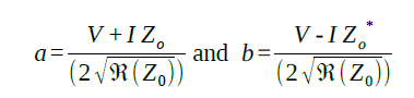
This wave-based behavior allows engineers to define incident and reflected/transmitted power waves that enter and exit a device under test.
Scattering Parameters themselves describe ratios of outgoing to incoming waves at the devices network ports where:
|a|2=incident power and |b|2=reflected ∨ transmitted power
More specifically,
So, the overall power delivered to the port is:
P=|a|2-|b|2
These S-Parameter ratios make up reflection and transmission coefficients based on power wave amplitudes instead of traditional forward and reverse voltage/current waves by assuming a complex characteristic impedance.
These ratios can also be expanded in a linear matrix relationship where:
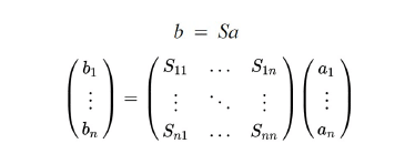
Each element in the matrix describes a relationship:
Sii: Reflection coefficient at port i
Sij: Transmission coefficient from port j to port i
Instead of writing N2 equations, one matrix equation expresses everything. This makes analysis of multi-port networks much easier and allows the use of linear algebra tools for network cascading, simulation, and design.
These power wave amplitude ratios are also used to display LogMag representations of reflection and transmission – leading to effective analysis for devices under test.
Before any S-Parameter measurements can take place on a device, a calibration needs to be performed to remove cable/fixture loss from the VNA to the DUT.
Calibration techniques such as SOLT and TRL further illustrate this plane wave dependence. These methods rely on known propagation constants and characteristic impedances to mathematically de-embed the measurement plane.
As mentioned before, the propagation constant is made up of phase shift and attenuation constants – values defined by the plane wave solution.
Characteristic impedance is just the balance of the electric to magnetic fields inside the medium between the conductors – also a plane wave defined concept.
While RF measurement systems appear to operate in the domain of voltages and power readings, they fundamentally rely on guided electromagnetic modes that arise from Maxwell’s equations under conductor-imposed boundary conditions. These guided waves can be understood as constrained solutions related to the plane-wave model.
When discontinuities exist in cables, fixtures, or calibration standards, reflected waves distort current distributions and can alter both conducted and radiated behavior in the larger system.
Poor calibration or impedance control does not merely affect numerical accuracy – it changes how electromagnetic energy is distributed throughout the structure.
Understanding measurements as wave interactions rather than simple voltage readings provides deeper insight into how test setups themselves can influence interference outcomes.
Conclusion
Here’s the big picture: the plane wave solution provides a closed-form description derived from Maxwell’s Equations, physical interpretation of electromagnetic energy flow, and a universal model that connects theory to RF hardware.
From transmission lines to antennas and measurement systems, the plane wave solution underpins modern RF design and compliance testing.
Understanding this foundation allows engineers to predict propagation, control reflection, and better interpret measurement results – reducing the likelihood that guided energy becomes unintended interference.