INTRODUCTION
EMC design guidelines have always been a popular subject in the EMC design community. What is the most important EMC design guideline, i.e. the guideline with the highest impact on the emission and immunity of electronic circuitry? Studying books and literature from renowned EMC experts often tells us that the most important EMC design guideline is:
- Minimize loop areas associated with high-frequency (HF) signal currents.
My preferred design guideline is another one. In this article we will show with an experiment demonstration that there is another design parameter that has much more impact on the EMC behavior of an electronic circuit than just the loop area of the signal current. Do you want to know which design parameter this is? Read on.
EXPERIMENT DEMONSTRATION

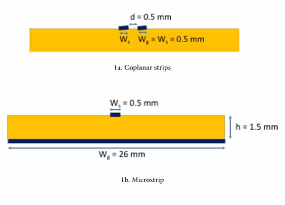
Figure 1. Printed Circuit Board configurations
The experiment demonstration consists of two configurations on a printed circuit board: a coplanar strips line and a microstrip line (Figure 1). Both lines have a length l = 100 mm. The coplanar traces have a width Wsignal = Wground = 0.5 mm. The distance between the two traces d = 0.5 mm. The microstrip has a trace width Wsignal = 0.5 mm. The width of the ground plane underneath the trace is Wground = 26 mm. The height of the trace above the ground plane is h = 1.5 mm. The copper thickness is 35 μm and the relative dielectric constant of the FR4 board material is εr = 4.7.
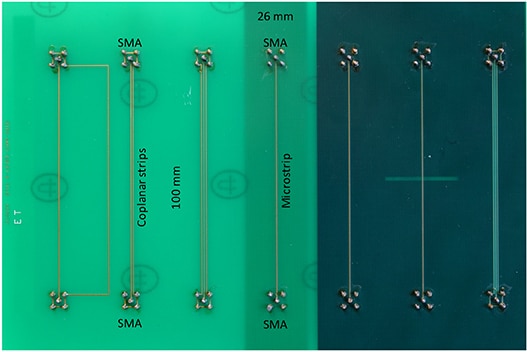
Figure 2 shows the demo board with the coplanar strips and microstrip lines.

Figure 2. Demo board with coplanar strips and microstrip lines
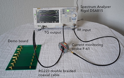
Figure 3 shows the measurement setup. On the demo board both lines are terminated with an SMA 50 Ω RF load. The input of the line is connected to the tracking generator output of the Rigol DSA815 spectrum analyzer with an RG223 double braided coaxial cable of 1 m length. The tracking generator output level is 100 dBμV (100 mV) over the frequency range 30 MHz to 300 MHz. For the frequencies involved the length l of the board traces is small compared to the wavelength (l << 1 m). In both lines flows a differential mode (DM) current IDM = 100 mV/50 Ω = 2 mA. With a current monitoring probe from Fischer Custom Communications (F-61) the common-mode (CM) current on the double braided coax cable is measured. The current probe is connected to the input of the spectrum analyzer. By shifting the current probe along the cable with the spectrum analyzer in the max hold mode the maximum CM current is recorded. The results will be discussed in the next section.

Figure 3. Measurement setup Common-Mode current generated by coplanar strips and microstrip
Now let’s have a look to the loop area of the high frequency signal current. For the coplanar strips line, the signal current loop area is approximately (taking the proximity effect into account) l × d = 100 mm × 0.5 mm = 50 mm2. The microstrip line has a signal current loop area l × h = 100 mm × 1.5 mm = 150 mm2. In our experiment demonstration the current loop area of the microstrip configuration is 3 times (10 dB) larger than that of the coplanar strips configuration.
At high frequencies (> MHz), signal currents take the path of least impedance, this is generally the path of least inductance, which is generally the path that minimizes the loop area. Currents return as close as possible to the path of the outgoing current. In the case of the microstrip most of the return current flows in the ground plane directly underneath the signal trace.
RESULTS AND DISCUSSION
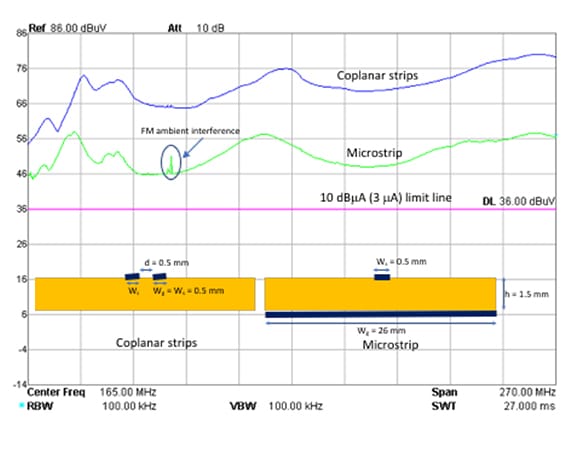
The measurement results of the maximum CM current for the co-planar strips and microstrip configuration are depicted in Figure 4. Over the full frequency range from 30 MHz to 300 MHz the co-planar strips line generates approximately 20 dB higher CM currents than the microstrip line, although its current loop area is 10 dB smaller. The CM current limit line of 10 dBμA (3 μA) shown in Figure 4 is based on the far field radiation of a resonant half wave dipole antenna and corresponds roughly with a maximum electric field strength of 30 μV/m (30 dBμV/m) at a 10-meter distance from the antenna (legal radiated emission limit). The current probe F-61 has a transfer impedance of 20 Ω in the frequency range 30 MHz to 300 MHz. So, a current of 3 μA will give at the 50 Ω input of the spectrum analyzer a voltage of 3 μA × 20 Ω = 60 μV = 36 dBμV.
What is the physics behind this CM current generation? The DM current IDM in the circuit loop on the board induces a CM voltage Vg across the ground return conductor. This CM ground voltage Vg acts as the antenna voltage for the cable connected to the board and generates antenna currents (CM currents) on the shield of the coax cable. The cable is an efficient antenna in the frequency range 30 MHz to 300 MHz and in the graphs in Figure 4 the cable resonances are clearly visible. The radiated emission is proportional to the antenna current (CM current).

Figure 4. Measurement results common-mode current coplanar strips versus microstrip
The CM ground voltage is determined by the partial inductance of the ground return lead: VCM = IDM2πfLg.
As a first order approximation for the partial inductance of a microstrip ground plane we can use the formula2:
Lg ≈ (μ0h)/(2Wg) if Wg >> h permeability μ0 = 4π10-7 (H/m).
The ground plane inductance Lg (Henry/m) is proportional with the trace height h (m) above the plane and inversely proportional with the ground plane width Wg (m).
For our microstrip configuration (h = 1.5 mm, Wg = 26 mm) the resulting ground plane inductance is:
Lg microstrip = 36 nH/m.
For our coplanar strips configuration (d = 0.5 mm, Wg = 0.5 mm) the inductance of the ground return trace is approximately:
Lg coplanar trace = 300 nH/m, i.e. an 18 dB higher inductance than that of the microstrip ground plane.
This difference of approximately 18 dB in ground return inductance is reflected in the CM current (radiated emission) plots of the coplanar strips and microstrip in Figure 4. The lower the ground return inductance the lower the radiated emission. In3 the theory of partial inductance to control emissions is explained very clearly.
CONCLUDING REMARKS
From the experiment we learn that although the differential mode current loop area of the microstrip line is much larger (10 dB) than that of the coplanar strips line the radiated emission of the microstrip line is much lower (20 dB) in the frequency range 30 MHz to 300 MHz. The main reason for this behavior is the partial inductance of the ground return lead. The ground plane of the microstrip has a much lower inductance than the ground trace of the coplanar strips, which results in a much lower common-mode ground voltage for the microstrip line and consequently a much lower radiated emission. The design parameter that has the highest impact on the EMC performance of an electronic circuit is not just the signal loop area but the partial inductance of the ground return conductor.
We may conclude that the most important EMC design guideline is:
- Minimize the inductance of the ground return conductor.
On a printed circuit board this can be realized by making the ground return conductor shorter, placing the signal trace closer to the ground plane AND by making the ground return plane wider. This is also valid for flex foil cables. The ultimate example of an extremely low ground return inductance (low transfer impedance) is an HF coax cable with a semi-rigid coaxial shield. This solid shield results in hardly any field leakage, assuming perfect connectors.
Do you have a different opinion? Let’s start a discussion! Contact Marcel at: marcel.van.doorn@home.nl.
REFERENCES
[1] https://learnemc.com/the-most-important-emc-design-guidelines
[2] F.B. J. Leferink, M.J.C.M. van Doorn, “Inductance of Printed Circuit Board Ground Planes”, IEEE International Symposium on Electromagnetic Compatibility, Dallas 1993.
[3] Glen Dash, “Know the Theory of Partial Inductance to Control Emissions”, IN Compliance, 2010 Annual Guide, www.incompliancemag.com


