As soon as current flows through metal conductors, inductance exists
Bruce Archambeault, Ph.D., IBM Distinguished Engineer, IBM,
Research Triangle Park, NC
The concept of inductance is one of the most misunderstood concepts in electrical engineering. Terms such as ‘self inductance’, ‘loop inductance’, ‘partial inductance’, ‘mutual inductance’ are used with little concern for the true physics behind the effects and causes of inductance.
Inductance is important to EMI/EMC design considerations since it is one of the primary limiting factors in high-frequency design. Whenever there is metal, and current flows though that metal, inductance is present and will affect the current flow. At high frequencies, this intrinsic inductance dominates all components, traces, and metal planes. Even capacitors and resistors become inductors.
A complete study of inductance would fill at least one entire book. The purpose of this article is to help the reader better understand the concepts of inductance, mutual inductance, and partial inductance as they apply to EMI/EMC design, especially on printed circuit (PC) boards.
Where’s the Loop?
One of the first things we learned in our first circuits class is that current must always return to its source. Usually we learn this initially for DC circuits, and then progress into AC circuits. However, by the time we start doing high speed circuit board design, many of us seem to forget this fundamental principle. Current must always flow in a closed loop, regardless of the frequency. As a printed circuit board designer, or an enclosure designer, or a system designer, you should always ask the question “How does the current return to its source?” Current must flow in a closed loop. Indeed, current will flow in a closed loop. The only real question is whether it will take a path that helps reduce EMI emissions, or a path that increases EMI emissions. It is much better to design a return current path ‘on purpose’ rather than ‘by mistake’. Without this intentional design of the return current path, engineers should also ask themselves “Do you feel lucky today?”
When someone talks about the inductance of a via, or a straight piece of wire, there is no loop so there is no inductance. In the case of a via, if there is no intentional return current via, then the return current will spread out and will flow through the dielectric as displacement current. The further the current travels, the larger the loop and therefore the larger the inductance. If a return via is placed nearby the signal via, then the inductance will change because the loop area has changed. As we move the return via closer, the loop area changes and so does the inductance of the original signal via. Clearly, the signal via by itself cannot have many values of inductance. The value of inductance of the loop where the via is part of that loop, determines the ‘via inductance’.
Faraday’s Law
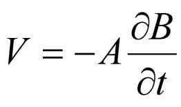
When the current in a loop changes with respect to time, the magnetic field associated with that current also changes. As this changing magnetic field cuts through a conductor, it induces a voltage in the circuit of that conductor. This change occurs whether the magnetic field lines cut through a different conductor or the same conductor as the original current. The voltage induced in a single wire loop is equal to the time rate of change of the magnetic flux passing through the wire loop.[1], [2] This is described in Faraday’s law of electromagnetic induction as:
(1)

Often equations such as (1) are not carefully examined for an intuitive understanding of the basic physics. Faraday’s law is not as complex as it might first appear. The right-hand side of (1) describes the amount of time-varying magnetic field within some area. The left-hand side of (1) is the definition of voltage (electric field along a path). And in this case, the path is a closed loop. The minus sign on the right-hand side indicates that the voltage will oppose the flow of current that created the magnetic field in the first place. This opposition is the basic definition of inductance. Notice that the left-hand side integral is a closed loop integral. Also notice the right-hand side is the amount of (time changing) magnetic field contained within an area. Naturally, to calculate an ‘area’, we must have a closed circumference, so both sides of this equation clearly indicate a closed loop is required to define inductance. Furthermore, the larger the loop area (right-hand side) is, the greater the inhibiting effect of inductance.
We can simplify (1) by considering the case of a simple square loop (shown in Figure 1). If the loop is small compared to the wavelength of the frequency of interest, then it can be assumed that the magnetic flux is constant over the area A, and Equation (1) can be reduced to
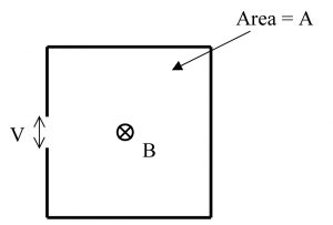
The amount of voltage induced from a time-varying magnetic field can be found for any geometry using Equation (1) and for a simple rectangular loop using (2). Again, it is clear that the larger the area in (2), the greater the inhibiting inductance.
Now that we have considered the basic definition of inductance, we can use some simple equations to find the value of inductance based on the physical dimensions of a loop. Assuming the loop area is much smaller than a wavelength over the frequency range of interest, the magnetic field is approximated as a constant. The approximate inductance for a few simple shapes[3] is given below.
Simple Round Loop
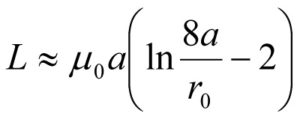
For a simple isolated current loop, where the wire radius r0 is much smaller than the loop’s radius a, then the loop’s inductance is approximated as
If multiple turns of the wire loop are used, then the inductance is simply multiplied by the number of turns to find the total inductance of the number of loops. Notice from (3) that the inductance is directly proportional to the loop area a, but only minimally affected by the wire radius r0 (because of the natural log function). Once again, the importance of the loop area to the inductance is clear.
Simple Square Loop
For an isolated square loop (with side length = w) in free space where the wire radius is much smaller than the loop area (r0 <<w2), the inductance can be found using
Simple Rectangular Loop
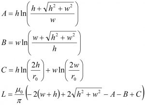
For a single turn rectangular loop in free space, the inductance can be found from
where
w = the width of the rectangle (wide dimension)
h = the height of the rectangle (short dimension), and
r0 = the wire radius.
While these formulas look complicated, they can be easily calculated with a spreadsheet program. Moreover, in each of these formulas, it is clear the loop area contributes significantly more to the value of the inductance than does the conductor size.
Why Do We Care About Loop Inductance?
One of the major concerns in EMI/EMC is inductance, especially the inductance of filter components. For example, capacitors are used on printed circuit boards (PCBs) for decoupling power/ground planes, I/O filter components, and other high frequency purposes. The inductance associated with the physical connection of the capacitor (mounted on the top/bottom of the PCB) to the appropriate planes will dominate the impedance of the capacitor at high frequencies and will make the capacitor ineffective at high frequencies. This inductance must be included in any analysis.
Accurate calculation of the inductance of a capacitor connection requires a complex formula.[4] However, since the inductance is directly proportional to the loop area, we can get a relative figure-of-merit by simply converting this complex problem into a simple rectangular loop and calculating the rectangular loop area for each option. If one option has less loop area, then it will have less inductance and will be the preferred design option.
Figures 2 and 4 show a low inductance decoupling capacitor connection, while Figures 3 and 5 show a high inductance decoupling capacitor connection.
In Figures 2 and 3, the loop area is much different, with the loop in Figure 3 significantly larger. For this example, where the power/ground plane is closer to the bottom of the board than the top, the loop area would be smaller (Figure 4), and the connection inductance would be lower if the capacitor were mounted on the back side of the board rather than the top side of the board. The opposite would be true if the power/ground plane pair were near the top of the PCB, as shown in Figures 2 and 5.
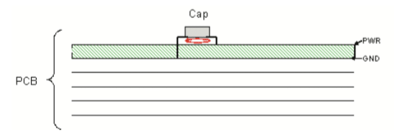

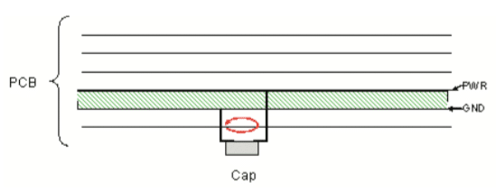

Table 1 shows some example values of the connection inductance associated with a PCB mounted decoupling capacitor for some typical dimensions. The more complex formula is more accurate, but even the simple rectangular formula values are accurate enough for most applications.

From Equation 5, it is important to notice that the wire radius has very little impact on the loop inductance, and the height and width (area of the loop) have the major impact on the value of the loop inductance.
This type of analysis is also valid to decide if special board technologies, for example, buried capacitance, are worth the cost for your board stackup configuration. If the buried capacitance layer is deep in the board (closer to the bottom), then the rectangular loop area between the IC power/ground pins and the buried capacitance layer will be high, minimizing any good effects from the buried capacitance layer. Alternatively, if the buried capacitance layer is near the top of the PCB, the rectangular loop area associated with the connection inductance is small, resulting in the IC receiving the benefit of the buried capacitance layer without significant connection inductance.
Mutual Inductance
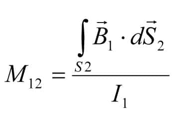
The mutual inductance of real world circuits is often difficult to calculate since the loops are seldom simple geometries, and other metal in the surrounding environment will affect the way the fields behave. If it is assumed that two loops are located in free space (electrically far from other conductors) then the problem is simplified and a reasonable estimate can be made. Under these conditions, the mutual inductance between the two loops is defined as
where
I1 = the current flowing in loop #1,
B = the magnetic flux created by the current in loop #1, and
S2 = the surface of loop #2.
In Equation (6) the magnetic flux from the current in the first loop is integrated across the surface of the second loop to find the mutual inductance. If the loops are small enough that we can assume the magnetic field is constant across the face of the loop, then the mutual inductance is simply the amount of magnetic flux from the first loop contained within the area of the second loop, and divided by the current in the first loop. Consequently, it is clear that the mutual inductance is determined by the size of the two loops and the way they are oriented with respect to each other. Larger loops will have more mutual inductance. Loops closer together will have more mutual inductance (since the magnetic flux from the first loop will be stronger). Loops with their faces oriented the same way will also have more mutual inductance (since the magnetic flux will be maximized).
Why Do We Care About Mutual Inductance?
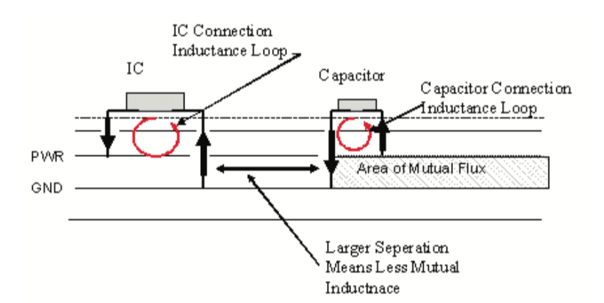
When a decoupling capacitor is placed close to the IC power pins, the area of mutual inductance can effectively lower the path loop inductance. For this reduction to be significant, the placement of the capacitor and IC must be close together.
Figure 6 shows an example of an IC and decoupling capacitor mounted on a PCB. When the via connections are as shown in Figure 6, the direction of the current in the two vias closest together results in magnetic flux in the opposite direction in the area of mutual flux between the power/ground planes as shown in Figure 6. This effect of opposite mutual inductance lowers the path impedance. This decrease in the overall inductance by this effect is seen only when the capacitor is very close to the IC.
Partial Inductance
The fundamental definition of inductance requires a current flowing in a loop. Without a complete loop, there cannot be inductance. Practical considerations, however, lead us to discuss the inductance of a part of the overall current loop, such as the inductance of a capacitor. This idea of discussing the inductance of only a portion of the overall loop is called partial inductance.[4], [5] Partial inductances can be combined to find the overall inductance using Equation (7).
(7)

Why Do We Care About Partial Inductance?
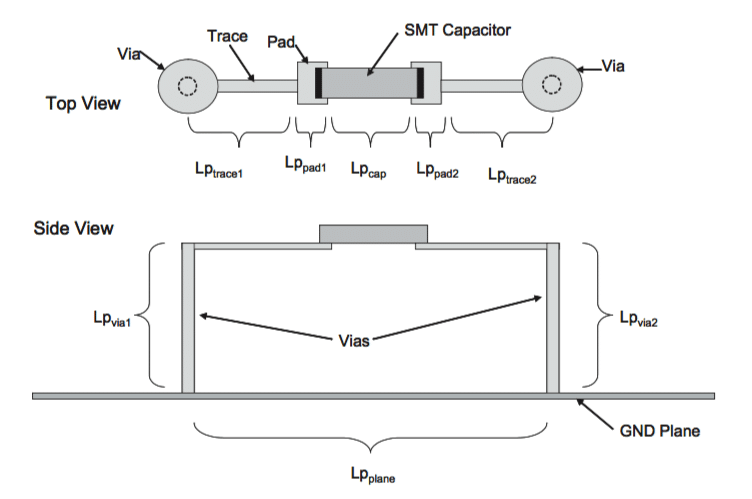
The concept of partial inductance is especially useful when the physical geometry is complex, or when the current is not uniform throughout the cross section of the metal. For example, Figure 7 shows a surface mount capacitor (SMT) on a PCB with connection vias, traces, etc. While a simple rectangular loop formula can be used to find an approximate loop inductance, the various conductor cross sections render the calculation only approximate. The concept of partial inductance can find each component’s partial inductance and can combine them at the end to find the total loop inductance as in Equation (8).
Using partial inductances, the total loop inductance would be given by

where Lp is a component’s partial inductance Lpm is the partial mutual inductance of the parallel components.
Note that the structure can be analyzed with the possible goal of reducing the total loop inductance. Each of the individual segments can be changed (for example via diameter increase) to determine the effect on the final inductance. Using this analysis, many ‘what if’ configurations can be quickly analyzed.
Summary
The basic principle that inductance requires current to flow in a loop is an important concept to understand. This is not unreasonable since current must flow in a loop. The size of the current loop determines the amount of inductance.
Inductance is a basic building block in electronic circuits—e.g., as soon as metal conductors are used and current flows through them, inductance exists. This inductance becomes the limiting factor in all high-frequency circuits. For example, when capacitors are used as filter elements or as decoupling capacitors, the loop inductance associated with the connection of that capacitor to the circuit board will limit the frequency range in which the capacitor is an effective component.
A brief discussion about mutual inductance and partial inductance is also given. However, the idea that a closed loop is required to estimate inductance also holds true for the mutual inductance and partial inductance calculations.
This has been a very brief introduction to inductance. A much more complete study of this subject is available in the references.
References
- J.D. Kraus and K.R. Carver, Electromagnetics, 2nd Edition, McGraw-Hill, 1973
- F.M. Tesche, M.V. Ianoz, and T. Karlsson, EMC Analysis Methods and Computational Models, Wiley-Interscience, 1997
- F.W. Gover, Inductance Calculations, Dover Publications, NY, 1946
- A.E. Ruehli, “Inductance Calculations in a Complex Integrated Circuit Environment,” IBM J. Research and Development, 16, pp 470-481, 1972
- C.R. Paul, Analysis of Multiconductor Transmission Lines, Wiley, 1994
Dr. Bruce Archambeault is an IBM Distinguished Engineer at IBM in Research Triangle Park, NC. He received his B.S.E.E degree from the University of New Hampshire in 1977 and his M.S.E.E degree from Northeastern University in 1981. He received his Ph. D. from the University of New Hampshire in 1997. His doctoral research was in the area of computational electromagnetics applied to real-world EMC problems.In 1981 he joined Digital Equipment Corporation and through 1994 he had assignments ranging from EMC/TEMPEST product design and testing to developing computational electromagnetic EMC-related software tools. In 1994 he joined SETH Corporation where he continued to develop computational electromagnetic EMC-related software tools and used them as a consulting engineer in a variety of different industries. In 1997 he joined IBM in Raleigh, N.C. where he is the lead EMC engineer, responsible for EMC tool development and use on a variety of products. During his career in the U.S. Air Force, he was responsible for in-house communications security and TEMPEST/EMC related research and development projects.Dr. Archambeault has authored or co-authored a number of papers in computational electromagnetics, mostly applied to real-world EMC applications. He is currently a member of the Board of Directors for the IEEE EMC Society and a past Board of Directors member for the Applied Computational Electromagnetics Society (ACES). He has served as a past IEEE/EMCS Distinguished Lecturer and Associate Editor for the IEEE Transactions on Electromagnetic Compatibility. He is the author of the book “PCB Design for Real-World EMI Control” and the lead author of the book titled “EMI/EMC Computational Modeling Handbook.”

