Soo Man (Sweetman) Kim, Vishay Intertechnology, Inc., Malvern, Pennsylvania, USA

A major challenge in automotive design is protecting electronics – such as control units, sensors, and entertainment systems – against damaging surges, voltage transients, ESD, and noise that are present on the power line. Transient voltage suppressors (TVS) are ideal solutions for automotive electronic protection and have several important parameters for these applications, including power rating, stand-off voltage, breakdown voltage, and maximum breakdown voltage. Following are definitions for these parameters.

POWER RATING
The power rating of a TVS is its surge-absorbing capability under specific test or application conditions. The industrial-standard test condition of 10 μs/1000 μs pulse form (Bellcore 1089 spec. [1]) is shown in Figure 1. This test condition differs from the TVS transient voltage absorbing capability test condition of 8 μs/20 μs pulse form, as shown in Figure 2.
BREAKDOWN VOLTAGE (VBR)
The breakdown voltage is the voltage at which the device goes into avalanche breakdown, and is measured at a specified current on the datasheet.
MAXIMUM BREAKDOWN VOLTAGE
(VC: CLAMPING VOLTAGE)
The clamping voltage appears across the TVS at the specified peak pulse current rating. The breakdown voltage of a TVS is measured at a very low current, such as 1 mA or 10 mA, which is different from the actual avalanche voltage in application conditions. Thus, semiconductor manufactures specify the typical or maximum breakdown voltage in large current.

STAND-OFF VOLTAGE (VWM): WORKING STAND-OFF REVERSE VOLTAGE

The stand-off voltage indicates the maximum voltage of the TVS when not in breakdown, and is an important parameter of protection devices in circuits that do not operate under normal conditions. In automotive applications, some regulation of the automotive electronics is provided by “jump-start protection.” This condition supplies 24 VDC in 10 minutes to 12-V type electronics, and 36 VDC in 10 minutes to 24-V type electronics without damage or malfunction of the circuit. Thus, the stand-off voltage is one of the key parameters in TVS for automotive electronics.
PRIMARY PROTECTION OF THE AUTOMOTIVE POWER LINE (LOAD DUMP)

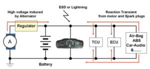
Automotive electronics, such as electronic control units, sensors, and entertainment systems, are connected to one power line. The power sources for these electronics are the battery and alternator, both of which have unstable output voltages that are subject to temperature, operating status, and other conditions. Additionally, ESD, spike noise, and several kinds of transient and surge voltages are introduced into the power and signal line from automotive systems that use solenoid loads, such as fuel injection, valve, motor, electrical, and hydrolytic controllers.

WHAT IS LOAD DUMP?
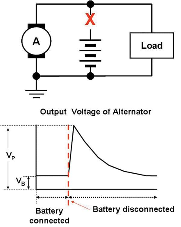
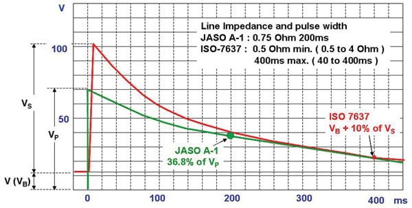
The worst instances of surge voltage are generated when the battery is disconnected when the engine is in operation, and the alternator is supplying current to the power line of the vehicle. This condition is known as “load dump,” and most vehicle manufacturers and industry associations specify a maximum voltage, line impedance, and time duration for this load dump status, as shown in Figure 5. The source impedance for load dump is higher than for the normal transient tests because the battery is disconnected and only the alternator, whose internal coil acts like a current limit resistor, is sourcing the power.
The following general considerations of the dynamic behavior of alternators during load dump apply:
a) The internal resistance of an alternator, in the case of load dump, is mainly a function of alternator rotational speed and excitation current.
b) The internal resistance Ri of the load dump test pulse generator shall be obtained from the following relationship:
Ri = ( 10 X Unom X Nact ) /
( 0.8 X Irated X 12,000 min -1 )
where
Unom is the specified voltage of the alternator;
Nact is the specified current at an alternator speed of 6,000 min-1 (as given in ISO 8854);
Irated is the actual alternator speed, in reciprocal minutes.
Two well-known tests simulate this condition: the U.S.’s ISO-7637-2 Pulse 5 and Japan’s JASO A-1 for 14-V powertrains and JASO D-1 for 27-V powertrains. In this section we review the application of TVS for load dump in 14-V powertrains.
SPECIFICATION AND RESULTS OF LOAD DUMP TESTS
The U.S.’s ISO-7637-2 Pulse 5 and Japan’s JASO A-1 tests for 14-V powertrains are simulated in Table 1.

Some vehicle manufacturers apply different conditions for the load dump test based on ISO-7637-2 Pulse 5. The peak clamped current of the load dump TVS will be estimated by the following equation:
Calculation for peak clamping current:
IPP= (Vin– VC) ⁄ Ri
where
IPP is peak clamping current
Vin is input voltage
VC is clamping voltage
Ri is line impedance

The current and voltage waveforms of Vishay’s SM5S24A in the ISO-7637-2 test of 87V Vs, 13.5V V batt., 0.75 Ohm Ri and 400ms pulse width as shown in Figure 7a.

In Figure 7b the clamped voltage and current of load dump TVS fail in the ISO-7637-2 test of 87V Vs, 13.5V V batt., 0.5 Ohm Ri and 400ms pulse width because the device was over-dissipated. The clamping voltage drops to near zero, and the current passed through the device is increased to the maximum allowed by the line impedance.

The maximum clamping capability of Vishay load dump TVS of ISO-7637-2 pulse 5 test condition with 13.5V Vbatt and 400ms pulse width is shown in Figure 7c. To prevent failure, such as that shown in Figure 7b, it is important to respect the maximum rating of the TVS.
PROTECTION AGAINST NEGATIVE-GOING TRANSIENTS AND REVERSED SUPPLY VOLTAGE
There are two kinds of load dump TVS for the primary protection of automotive electronics: epitaxial and non-epitaxial. Both product groups have similar operating breakdown characteristics in reverse bias mode. The difference is that epitaxial TVSs have low forward voltage drop (VF) characteristics in forward mode, and non-epitaxial TVSs have relatively high VF under the same conditions. This characteristic is important to the reverse voltage supplied to the power line. Most CMOS ICs and LSIs have very poor reverse voltage capabilities.


The gates of MOSFETs are also weak in reverse voltage, at – 1 V or lower. In the reversed power input mode, the voltage of the power line is the same as the voltage of the TVS VF. This reverse bias mode causes electronic circuit failure. The low forward voltage drop of EPI PAR TVSs is a good solution to this problem. Another method to protect circuits from reversed power input is utilizing a polarity protection rectifier into the power line, as shown in Figure 8. A polarity protection rectifier should have sufficient forward current ratings, and forward surge and reverse voltage capabilities.
SECONDARY PROTECTION OF THE AUTOMOTIVE POWER LINE
The primary target of protection circuits in automotive systems is high surge voltages, but the clamped voltage is still high. Secondary protection is especially important in 24- V powertrains, such as found in trucks and vans. The main reason for this is the maximum input voltages for most regulators and dc-to-dc converter ICs for automotive applications are 45 V to 60 V. For this kind of application, using secondary protection, as shown in Figure 9, is recommended.
Adding resistor R onto the power line reduces the transient current, allowing smaller power-rating TVSs as the secondary protection. Current requirements for microprocessor and logic circuits in electronic units are 150 mA to 300 mA, and the minimum output voltage of a 12-V battery is 7.2 V at -18°C, or 14.4 V for a 24-V battery under the same conditions. In a 24-V battery under the above conditions, the supply voltage at a 300-mA load is 8.4 V at R = 20 Ω, and 11.4 V at R = 10 Ω at a minimum voltage of 14.4 V (24-V battery voltage in – 18 °C).
VL = (Vmin⁄ (Vmin⁄ IL)) × ((Vmin⁄ IL) – R)
where
VL is voltage to load
Vmin is minimum input voltage
IL is load current
R is Resistor value
Power rating of R = I2R
This supply voltage is higher than the minimum input voltages for most voltage regulators and DC/DC converter ICs to avoid wrong operation of circuit by low voltage input.
While safety and reliability issues are important considerations in automotive systems, they are beyond the scope of this article.
CONCLUSION
In this article, we’ve described all the transients and their modes that can damage automotive electronic systems. We’ve gone on to discuss the important parameters of TVSs, and have demonstrated that with the appropriate specifications, these devices can protect circuits against all transients and the load dump condition.
REFERENCES
[1] Bellcore 1089, https://www.scte.org
[2] ISO/DIS-7637-2.3 2004 Road vehicles – Electrical disturbances from conduction and coupling – Part 2. Electrical transient conduction along supply lines only. www.iso.ch
[3] JASO D 001-94 Japanese Automobile standard, http://www.jsae.or.jp
[4] ES-XW7T-1A278 – AC Component and Subsystem Electromagnetic Compatibility, Worldwide Requirements and Test Procedures, Ford Motor Company, http://www.fordemc.com
[5] IEC 61000-4-5 International Standard Electromagnetic Compatibility (EMC) – Part 4-5: Testing and measurement techniques, surge immunity test. www.iec.ch
ABOUT THE AUTHOR
Soo Man (Sweetman) Kim studied electronic engineering at YoungNam University in Korea and has worked for Vishay General Semiconductor on field application engineering and product marketing applications for rectifier and TVS devices since 1987.


