The engineer had found the use of a capacitor on a specific trace would solve a radiated emissions issue. However, placement on the connector where we put the capacitor during engineering work was not a production solution. So, the capacitor which was moved less than 1 inch away from the connector and turned sideways to fit on the circuit board. However, this degraded the emission results several dB and increased it above the limit. How could that be? They were identical on the schematic.
It has been said that the field of EMC is the design of circuits which consider things that do not appear on a schematic. These are the parasitic elements, the electric and magnetic field created by the circuit and coupled into adjacent circuits, wires, and components, and issues of unknown or uncontrolled current paths. To control these issues, it requires being aware of these fields, how they are generated, and the mechanism by which they couple, as well as how currents are generated and how they return to the source of the energy which created those currents.
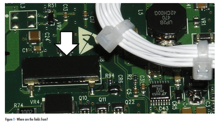
When EMI problems occur, they are often due to unknown or unforeseen issues of components. Take the following for example: In Figure 1, if there is a concern with cross coupled fields, we may want to reroute that white cable we see over the circuit board. Or maybe we would have concerns about the large inductor in the upper right corner, or the small one in the lower right under the cable. These may have uncontrolled magnetic fields which could couple energy into nearby traces. When testing was performed, neither of these were a problem. However, the conducted emissions measurements were over limit.
The issue arose from a DC-DC converter located to the left, and indicated with the arrow. This converter contains an internal transformer. The fields from this device ended up coupling into the input power trace running under the near side of the device indicated in this picture. Due to a misplaced filter, which was not located next to the input connector as it should have been, the input power conducted emissions increased by 20 dB and more due to the proximity of this converter and internal transformer. Rerouting the trace away from this converter improved the results radically (see Figure 2).

The cause of this issue was due to magnetic field coupling. Uncontrolled magnetic fields from the converter’s internal transformer could couple into an adjacent trace, which induced a current in that trace at the switching frequency of the converter, and higher harmonics of that frequency. The specification for this component shows performance with a wide margin with respect to conducted emissions limits. And the power to the device may have been compliant by itself. However, due to the fields generated by the device, noise was allowed to be reintroduced into the trace in an uncontrolled manner.
These magnetic coupling issues are usually found in lower impedance circuits where currents can flow with greater ease. But what happens in high impedance circuits? These are more susceptible to capacitive coupling. One way to demonstrate that is using a standard MIL-STD 461 or DO-160 setup.
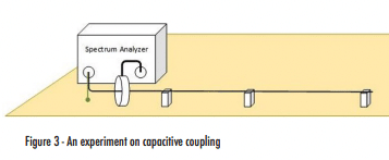
I took an inexpensive spectrum analyzer with a tracking generator. A tracking generator is an internal signal source that creates a signal at a set amplitude and the same frequency the analyzer is measuring. I ran the tracking generator signal into an unterminated 5-foot wire (150 cm), and the return signal was routed to a ground plane. A current probe was placed on the drive end of the wire. A simplified setup drawing is shown in Figure 3.

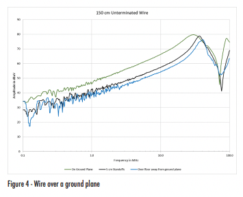
The figure shows the wire on 5 cm standoffs, as is commonly used for military and aerospace tests. For a second test, the wire was routed directly on the surface ground plane, and a third run with the wire routed the wire off the ground plane so that it was in space (held up with a plastic stand to avoid other parasitic coupling). The wire was swept with a signal from 100 kHz to 100 MHz. Only the wire was moved during the three scans, and no other changes were made to the setup, and the current probe was as close to the output port as physically possible. The results are shown in Figure 4.

Please note the following: At 10 MHz the induced current in the wire on the ground plane was 9 dB higher than the same wire on 5 cm standoffs, and 12 dB higher than the wire routed into “space”, away from the ground plane. Above 30 MHz, this system starts to break down, likely due to the cross coupled energy at the source, the line impedances (inductance), and other setup parasitic elements. However, up to 30 MHz, the results were repeatable.
So, what does this tell us? First, there is some coupling of energy from wires on 5 cm standoffs over a ground plane.
That should not surprise most experienced military and aerospace test engineers. This is also how the wires are routed in most military and aerospace applications which often have wires over a metal structure. Also note that unterminated wires closely coupled to conductive surfaces can capacitively couple their own return path. Remember this is an unterminated wire, so I did not allow a connection to the ground plane to close the current loop. The loop is closed by displacement currents, a time varying electric field due to the voltage difference between the wire and the ground plane (which was the return). And as physicists will state, “displacement currents play a central role in the propagation of electromagnetic radiation, such as light and radio waves.”1
When a cable inside equipment should avoid radiating on to a sensitive circuit, when possible route the cable near a conductive surface, such as a chassis. In doing so, the conductor can couple more energy into the chassis instead of the circuit, and preferably route the induced return current back to the source in a controlled manner. Conversely, if that cable is sensitive to having energy picked up from high energy or noisy circuits or systems, routing the cable along the conductive surface will help minimize the energy induced or coupled onto it. This comes from Gauss’s Law, the concept that parallel electric fields at the surface of a perfect conductor go to zero.
When a cable inside equipment should avoid radiating on to a sensitive circuit, when possible route the cable near a conductive surface, such as a chassis. In doing so, the conductor can couple more energy into the chassis instead of the circuit, and preferably route the induced return current back to the source in a controlled manner. Conversely, if that cable is sensitive to having energy picked up from high energy or noisy circuits or systems, routing the cable along the conductive surface will help minimize the energy induced or coupled onto it. This comes from Gauss’s Law, the concept that parallel electric fields at the surface of a perfect conductor go to zero.
An area often neglected is the issue with chassis bonds. A common method of determining the quality of a shield was to consider the material conductivity, the thickness, and the screw spacing. The conductivity along with the thickness will provide the maximum capability of the material to shield. If it is not conductive enough, or thick enough, you may never get the desired results.
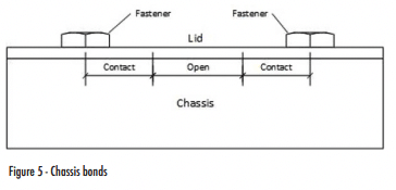
Now considering the screw spacing. A concept used for spacing is the amount of contact surface as shown in Figure 5. This concept is that contact occurs for the first third of the spacing between fasteners, and again for the last third, but the middle third is open.
Some of these “rules of thumb” do not consider the stiffness of the materials, the spacing of the fasteners, nor the coatings. For example, a steel box with a sheet metal lid that is 50 cm wide and only has fasteners in the corners, the likelihood of gaps in the middle of the seam is rather significant. There is not enough rigidness in the lid to maintain a bond in the middle. In this case, fasteners may need to be 5 to 10 cm apart to assure a bond. But with a thick-walled chassis that has a thick lid, the spacings between fasteners may be a bit wider and still maintain the bond. And yet the whole thing can go to waste if there is a coating on the chassis.

If one only looks at the potential opening, or window created between fasteners, as the driving factor in shielding effectiveness, you may miss a critical aspect of shielding. For the sheet metal box with 50 cm spacing, if the window is the full 50 cm, that relates to the half wavelength of the leakage. The shield would become effective below 300 MHz. If we reduce the spacing to 5 cm, the shield should be 20 dB better across the frequency range. Yet often that is not the case.
In one situation, the unit under test had a thick-walled chassis made of aluminum, with fasteners about 5 cm apart. The emissions found were from 1-10 MHz and failed the MIL-STD 461 limit imposed. In this frequency range, the aluminum chassis should have a shielding effectiveness well over 100 dB. The important item noted was that the emissions did not change much when the lid was off. And it was found the emissions were not from the cables. However, when the engineer cleaned off all the oil and grease buildup on the chassis and lid from the handling and construction of the unit, the emissions dropped 20 dB and passed the test.
In this case, the unit under test was a power supply with significant currents flowing internally and several magnetic cores inside. The resulting fields from the magnetic fields of the wiring, traces, and inductors and transformers, induced currents in the aluminum chassis under and around the circuit board, and then over the lid of the chassis. Once these currents start to flow, they need to complete a loop. When the induced currents reached the seam, they met an impedance which prevented the flow of the current directly. This created a voltage between the lid and the chassis. Voltages between two pieces of metal are in essence antennas and tend to transmit their energy. This may have been viewed as a transfer impedance problem, or the creation of displacement currents across the seams. The impedance between these metal parts could have been due to insulating materials (dirt, grease), too thin to transmit radio frequencies through it from inside to outside the chassis. However, if currents cannot flow across the gap, even that small, then the resulting voltages on the two sides of this barrier will then transmit the energy.
Note that not all issues are from internal components, circuits, or even the equipment under test itself. In one situation, a large medical device was found to have emissions from 150 MHz to 250 MHz whenever a specific circuit was energized. Several engineers and technicians tried to solve the issue over months. When an EMC consultant was finally called in, the consultant asked about an external power supply used to power the circuit in question. It turned out the power supply had very intense radiated emission issues due to diodes used in the switching power supply, however nobody had bothered to verify that external source.
When trying to capture all the relevant issues concerning EMC on a schematic, it is very difficult to consider all aspects that will arise. They do not provide DC to DC converters with magnetic field maps, and often will not caution the user concerning induced field alongside the component. And inductors are best modeled with capacitance across them which represent the capacitance of the windings. Capacitors should be modeled with inductors in series to represent the lead or trace inductance. Wires and traces include a bit of both aspects. And diodes are well established noise generators over 30 MHz now.
As EMC engineers, we need to be proficient in several disciplines, in many fields of engineering, to fully support the engineers we work with. Schematics will only tell you part of the story. Many parasitic elements are not documented. Mechanical and manufacturing techniques play a role in passing EMC requirements. Maintain an open mind, considering the unlikely, and expect the unexpected. Or in the words of Sherlock Holmes, “When you have eliminated all which is impossible, then whatever remains, however improbable, must be the truth.”2
References
1Encyclopedia Britannica, https://www.britannica.com/science/displacement-current
2 The Casebook of Sherlock Holmes (1927), The Adventure of the Blanched Soldier, by Sir Arthur Conan Doyle.


