Optimal shielding helps meet the challenges of cramming maximum functionality into minimal PCB space.
Paul J. Stus
Laird Technologies, St. Louis, MO, USA
Advances in the miniaturization of electronic components has intensified the need for manufacturers to solve multiple problems simultaneously and earlier in the design process. Solving the issues quickly and early in the design phase of a project will save time and money in manufacturing and will accelerate time to market.
In today’s electronic world, consumer devices requiring integration of wireless, video, audio, and storage technologies are the norm. However, as more components are packed onto boards to produce the advanced functionality required by modern users, substantial heat and EMI issues are being created, along with less space in which to solve the problem. Hence, EMI and thermal engineers are challenged to diagnose and resolve the common causes of slower operating speeds, component failures, and thermally induced stress.
If the EMI and heat issues found in today’s newer, smaller, faster, wireless, and highly productive products were rendered into a formula, it would read:
Noise + Heat = Problems
What then are the common goals of these engineering groups? How can different engineering groups align resources and work together to reduce thermal stress and EMI emissions, to pass internal reliability requirements, and to increase product life while enhancing the overall system?
In reviewing electronic component designs, all engineers need to be aware of the potential thermal and EMI issues. EMI can be found in almost any of today’s devices becaue of the use of microprocessors, RF chipsets, voltage regulators, and other integrated circuits (ICs), also known as IC chips, a widely used design option characterized by high frequencies. Typically, these issues are dealt with at the source and as close to that source as possible with board level shielding (BLS).
When it first became clear that thermal issues could impact the reliability of systems, designers often turned to a thermal interface material and heat sinks to enhance the heat dissipation. However, these components add weight and cost to the system, and many of the newer and smaller applications simply do not have the space for a heat sink. Ideally, designers would like to decrease the component count on the board. Additionally, designers want to protect the device from EMI at the board level, closest to the source where heat needs to be removed and where board level shielding is also required.
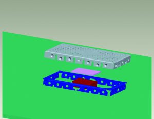
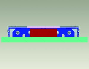
So what is a realistic, effective way for engineers to deal with the noise and heat of today’s electronics? A new approach for simultaneously reducing heat and EMI noise would be to apply a thermal interface material (TIM) to the board level shielding. By adding a thermal interface material, like that in Figure 1, the heat is more efficiently transferred from the IC to the large metal surface of the board level shielding. This heat dissipation would be enhanced by adding a second thermal interface material between the board level shielding and a second, larger heat spreader (Figures 2a, 2b, and 2c).
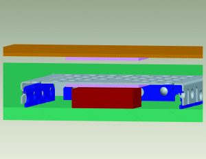
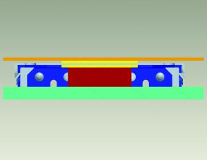
In some instances, the board level shielding may provide a large enough surface to dissipate the heat from the IC. Only testing of the application can determine if the board level shielding can provide enough heat dissipation or if a larger heat spreader will be needed.
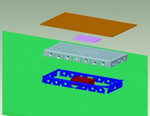
A common mistake in managing the heat from integrated circuits is not putting a thermal material between the IC and the board level shielding. If a thermal interface material is not placed between the board level shielding and the integrated circuit (Figure 3), the excess heat created by the integrated circuit is not directly removed. Instead, the heat simply radiates into the air gap, and the metal of the board level shielding has little effect on heat dissipation. This excess heat creates a problem because air is a very good thermal insulator and does not directly transfer heat. Without the thermal interface material, the IC will retain heat, will reach higher temperatures, and consequently, may not function properly.
Conversely, by adding the thermal interface material between the board level shielding and the integrated circuit, an engineer can actually take advantage of the metal of the board level shielding as a heat spreader. The thermal interface material eliminates the air gap and efficiently transfers heat from the IC to the board level shielding. The metal of the board level shielding then effectively provides an expanded surface area for heat dissipation.
The most common reason semiconductors fail is heat. Not only do high temperatures destroy devices. Even operation at elevated, non-destructive temperatures can degrade useful life. Data sheets specify a maximum junction temperature, which is typically between 100° C and 200° C for silicon. Most transistors have a maximum junction rating of 125° C, which is the temperature of the chip itself. The safe package temperature is much lower.
If thermal management is not considered, ICs will have shorter lives or will become less reliable. Excessive heat above the operating temperatures will burn out or will start destroying the delicate silicon structures inside the integrated circuits. All ICs have specified operating temperature ranges. When an IC operates above this range, the IC begins to fail. To achieve proper operating temperatures, heat dissipation considerations are included as part of the integrated circuits or product testing. Recommendations may be provided by the manufacturer of the IC, but not all applications are created equal.
CONCLUSION
There is no single way to protect products from EMI and heat. Still, by considering both issues earlier in the design process, costly problems in product testing can be avoided. Convergence technologies, or products that combine two products such as EMI and thermal into one product, can provide an attractive solution. Considering both EMI and thermal issues early in the design process can help eliminate costly problems later in the product development process.
Paul J. Stus is the global business director for the EMI strategic business group at Laird Technologies. He is currently responsible for developing, implementing and managing global business growth objectives, strategies and P&L for Laird Technologies’ EMI business unit. Stus joined Laird Technologies in 1997 as global technology manager. He led the development and launching of new products and processes globally. He has consistently been promoted throughout the Laird Technologies’ organization and has held positions such as global product director and director of sales. Prior to Laird Technologies, Stus began his career at Monsanto Company, where he worked his way from process engineer to operations unit leader to senior research engineer. Stus graduated from Wayne State University with a BS in chemical engineering and has an MBA from Washington University.
