Simple square wire loops may be well suited for injecting signals into circuit boards by inductive coupling.
Douglas C. Smith, D.C. Smith Consultants, Los Gatos, CA
CONSTRUCTION DETAILS
Square magnetic loops are very useful troubleshooting tools. This article will describe the construction and characteristics of shielded magnetic loops and compare them to unshielded magnetic loops made from stiff wire.
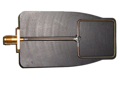
Figure 1 shows a square shielded loop built into a plastic housing, which has been split to show the loop inside. The electrical construction of the loop is described in [1]. For our purposes, one can think of the loop as starting with a straight length of semi-rigid coax of small diameter with an SMA connector on one end and shorting the center conductor to the shield with solder at the other end. Then the loop is bent around to form a square (being careful not to bend the coax too sharply at the corners) and the solder shorted end is soldered back on the coax so as to form a square symmetric loop. A small gap is made in the shield in the middle of the side opposite the feed line. A close up of the loop in Figure 1 is shown in Figure 2.
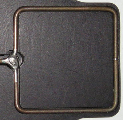
The gap in the shield can be seen in the middle of the right side of the loop. As shown in [1], shielding against electric fields is best achieved if the field is symmetric around a line from the solder junction to the gap in the shield, a condition that is met when a shielded loop is used to measure a field much further from a source than the size of the source itself. To help insure electric field symmetry when the loop is used on the surface of a circuit board in the near field, the gapped side should be held against the board with the loop itself perpendicular to the board. And therein lies the main reason for using a square loop; most circuit boards are flat and one side of the loop can be held directly against a circuit board resulting in better coupling to the circuit than a round loop of the same size would give.
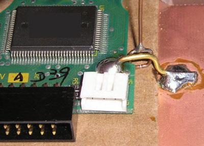
Figure 3[2] shows a small square shielded loop held next to a connection between a circuit board and the underlying “chassis.” In this case, there is coupling from all four sides of the loop into the circuit to achieve maximum coupling.
One can minimize the work required to build a shielded loop by buying a short length of small semi-rigid coaxial cable with SMA connectors already mounted on each end. The assembly can be cut in half to make two shielded loops saving the trouble of mounting the connectors on the semi-rigid cable. The smaller the semi-rigid coax diameter, the better coupling between the center conductor of the coax and the adjacent circuit.
I use square shielded loops both to measure many kinds of signals and to inject small RF signals (~0 dBm) into circuits. Some of my techniques involve coupling high voltage/current short pulses into a circuit[3]. I do not recommend shielded loops made from small semi-rigid coax for this purpose because of possible voltage breakdown in the coax and even heating under some conditions. For large pulses, I use unshielded stiff wire loops.
PARASITIC COUPLING
(Electric field shielding of magnetic loops is not always effective)
Shielded magnetic loops are used to reduce electric field coupling to the loop and square magnetic loops are useful for coupling signals into a PCB or measuring noise in a circuit. However, significant electric field coupling can still occur with shielded loops. One case of electric field coupling between a pair of shielded loops is presented, which results in a significant resonance between the shielded loops. Such a resonance can cause errors in signal injection used for troubleshooting circuits.
Figure 4 shows an overall view of the test comprised of a pair of square shielded loops connected to a spectrum analyzer set up to perform a two port insertion loss measurement. The two loops are positioned end-to-end and held in place with paper tape on the back of the loops. A close-up of the two loops is shown in Figure 5. The semi-rigid coax used to form the loops is encased in the plastic seen in the figures.
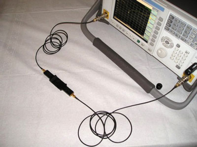

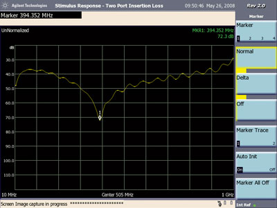
Figure 6 shows the resulting plot of insertion loss (unnormalized) between 10 MHz and 1 GHz. Notice the significant dip of around 30 dB at about 394 MHz. This feature has the appearance of a resonance that can be explained with reference to Figure 7.
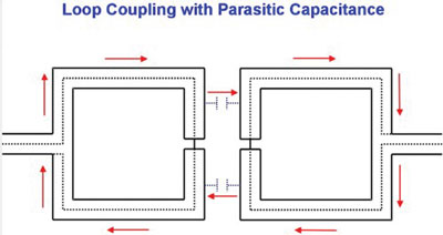
The capacitance between the shield segments shown in Figure 4 form a resonant circuit with the inductance of the two loops. The current path for the resonance is shown by red arrows. The loops I used were one inch on a side, so the effective loop for the resonant circuit is approximately two inches by one inch. The Missouri University of Science and Technology inductance calculator[4] gives an inductance of about 125 nH for such a loop assuming a wire (shield) radius of 10 mils. The resonant frequency of 394 MHz then yields a capacitance of about 1 pF for the total capacitance in the tuned circuit of Figure 4. But how is energy coupled into this resonant circuit? There are a number of ways to explain how this happens, but the important point is that it does happen. Adding ferrite to the coax cables feeding the loops did not change the characteristics of Figure 3 so the current loop of Figure 4 is the controlling feature.
One possible simplified explanation is as follows: Current flowing in the center conductor of the driven loop generates inductive voltage drop (Ldi/dt) around the loop. A shielded cable is nearly an ideal transformer, so the voltage drop on the center conductor under each of the two shield segments is magnetically coupled into the shield segments as Mdi/dt. The mutual inductance, M, between the center conductor and the shield, is the inductance of the shield itself. This driving voltage on the two shield segments causes current to flow around the four shield segments coupled by the parasitic capacitance between the loop shields as shown in Figure 4 thus driving the resonant circuit. In this discussion, I am treating the circuit as composed of lumped elements since each segment and the loops themselves are small compared to a wavelength at 400 MHz.
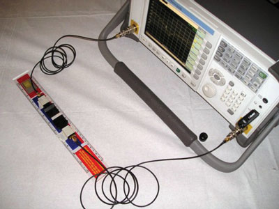
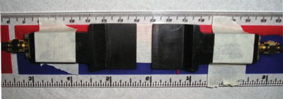
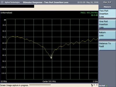
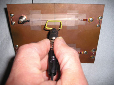
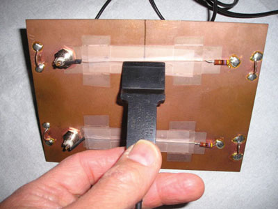
If a resonance caused by the current path of Figure 7 is the reason for the dip in plot in Figure 6, then moving the loops apart should increase the resonant frequency. This would happen because the capacitance between the loops is reduced. Figure 8 shows the test setup modified to space the loops one cm apart. The two loops are taped to a plastic ruler to maintain the spacing during the measurement. A close-up of the spaced loops is shown in Figure 9.
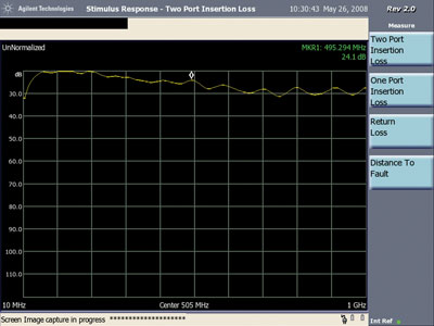
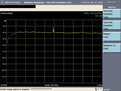
The resulting two port insertion loss plot is shown in Figure 10. Note that the resonant dip has moved to about 495 MHz. This would represent a significant drop in capacitance on the order of 40%.
As the loops are moved further apart, the capacitance between all parts of the loops begin to contribute an increasing portion of the capacitance between the loops complicating the picture somewhat. One would not expect the capacitance to decrease as much as just that of the facing sides as the loops are separated.
This effect can result in errors during troubleshooting a circuit using signal injection. The problem is that using a shielded loop can sometimes give a false sense of security that electric field effects are not important.
PARASITIC COUPLING BETWEEN UNSHIELDED WIRE LOOPS
Unshielded wire loops are inexpensive and easy to build. However, capacitive (E field) coupling has always been a concern when using these simple loops. Coupling between unshielded wire loops is investigated, included parasitic capacitive coupling. Performance is compared to shielded loops and the simple unshielded wire loop is shown to be superior in some cases to shielded loops.

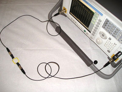
Figure 11 shows an overall view of the test setup comprised of a pair of square wire (unshielded) loops connected to a spectrum analyzer set up to perform a two port insertion loss measurement. The two loops are positioned end-to-end. A close-up of the two loops is shown in Figure 12. The loops are about one inch, a few cm, on a side.
In Figure 12, the loops are reversed in position, that is the + side of one loop (center conductor of BNC) is opposite the – of the other loop (ground side of BNC). This will be referred to as the “reversed” direction. By inverting one of the loops in Figure 12 the “normal” direction is obtained (+ side to + side of the loops). Data is presented for both directions. Capacitive coupling between the loops would cause the normal and reversed positions of the loops to yield different responses or cause resonant responses.

If only magnetic field coupling existed between the loops, the change resulting when one of the loops is reversed would be a 180 degree phase shift in the output, which would not change the spectrum analyzer plot. If significant capacitive coupling existed between the loops, the output of the receiving loop would be the combination of the inductive and capacitive components. Since the phase of the inductive component is reversed when one loop is reversed but the phase of the capacitive component is not, the spectrum analyzer plot will be different.
Figures 13 and 14 show the loop-to-loop transmission from 10 MHz to 1 GHz for the reversed case and normal cases of the two loops as explained above. As discussed above, the loop-to-loop transmission for a pair of shielded loops in the end-to-end configuration contained a deep resonance of about 30 dB due to inter-loop capacitance. Neither Figure 13 or Figure 14 shows such a resonance, with the frequency response being relatively flat by comparison. The differences between Figure 13 and Figure 14 are about 6 dB maximum at a few frequencies and the traces are not as smooth as the shielded loops. However the “lumps” in the frequency response in Figures 13 and 14 are only a few dB in peak amplitude, much smaller than the 30 dB resonant dip seen in the shielded loop case discussed above.
The relatively flat frequency response in Figures 13 and 14 are indicative that simple wire loops may be useful for injecting signals into circuit board paths and cables by inductive coupling.
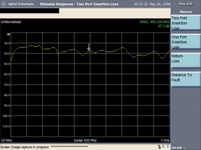

Figure 15 shows the overview of a related case where the loops are overlapped to insure maximum coupling. Figure 16 shows a close-up of the loops. Notice in Figure 16 that the loops are arranged in the normal position as opposed to reversed in Figure 12, that is the side of the loops connected to the BNC center pin (or shield connection) are both on the same side.

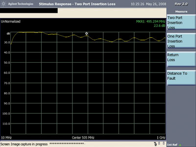
Figures 17 and 18 show the coupling from 10 MHz to 1 GHz for the setups of Figures 15 and 16 in both the normal and reversed orientations. The difference between the two traces is only a few dB, and without shielding. The response curves look very close to the response of shielded loops that are overlapped, within a few dB.
COUPLING TO A PCB
(From shielded and unshielded magnetic loops)
Shielded loops are often used to minimize electric field (capacitive) coupling. A case is shown where using a shielded loop to inject signals into a path on a circuit board results in a significant resonance whereas using an unshielded wire loop results in a relatively flat frequency response of the injected signal. Unshielded wire loops are thus shown to be more useful than shielded loops in some cases.
Figure 19 shows a square unshielded wire loop held up to a path crossing a break in the ground plane of a test board that is used for many of my experiments. The injected signal was measured at the BNC connector on the board (left side) for the cases where the loop is positioned as shown and for a 180 degree rotation of the loop and similarly for a square shielded loop (embedded in plastic for strength) as shown in Figure 20.
Figures 21 and 22 show the measured signal at the BNC connector on the board for the unshielded wire loop in the normal position (as in Figure 1) and for the 180 degree rotated position of the loop respectively. The data was taken using a spectrum analyzer as a two port insertion loss measurement. The square loop was connected to the tracking generator output and the BNC connector on the board was connected to the receiver input of the analyzer.
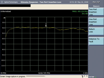
Capacitive coupling between the loop and the board will cause either a resonance effect (dip or peak in the response) or a directional effect when the loop is rotated 180 degrees because the phase of the inductive coupling changes by 180 degrees whereas the capacitive coupling remains the same. As can be seen in Figures 21 and 22, there is no resonant effect, the frequency response is nearly flat. The capacitive coupling itself is very low compared to the inductive coupling because the difference between Figures 21 and 22 is only a few dB and then only at the higher frequencies above 600 MHz. Contrast the responses in Figures 21 and 22 for the unshielded loop to the responses in Figures 23 and 24 for the shielded loop.
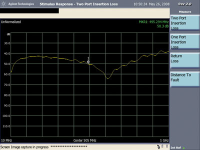
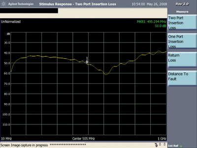
In both Figures 23 and 24, a resonant dip in the response is seen similar to that shown for coupling between shielded loops. In this case, the resonance is due to the sum of the inductance of the shields of the loop and the inductance around the split in the ground plane interacting with the capacitance between the shields and the ground plane of the board. As one would expect for a shielded loop, the plots in Figures 23 and 24 are not very sensitive to the normal and rotated positions of the loop.
One can conclude from the plots that the unshielded loop works better for injecting signals into a path crossing a ground plane split than does the shielded loop. I suspect this result holds in general for injecting signals into circuit boards with ground and power planes.
MEASUREMENTS IN THE TIME DOMAIN
(For shielded and unshielded magnetic loops)
Shielded loops are often used to minimize electric field (capacitive) coupling. A case is shown where using both unshielded and shielded magnetic loops to inject signals into a path on a circuit board results in an injected signal that is about the same for both loops. Unshielded wire loops are thus shown to be as useful as shielded loops for pulse injection.
Figure 25 shows a square unshielded wire loop held next to a path crossing a break in the ground plane of a test board that is used for many of my experiments. The injected signal from a TG-EFT pulse generator connected to the loop was measured at the BNC connector on the board (left side) using an oscilloscope for cases where the loop is positioned as shown and for a 180 degree rotation of the loop. A similar test was done using a square shielded loop as shown in Figure 26 (see Figure 20 above). Bandwidth of the oscilloscope used was 500 MHz and the TG-EFT was set to generate open circuit pulses of 100 Volts with a risetime of about 2 ns and a pulse duration of about 100 ns. Figure 27 shows the TG-EFT pulse generator.
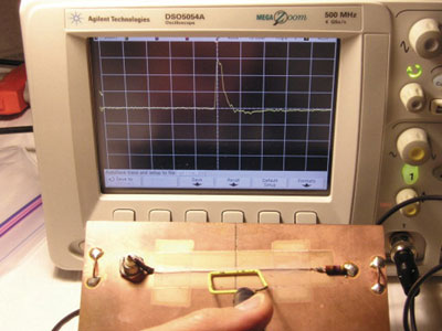

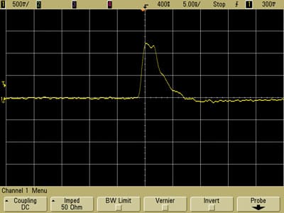
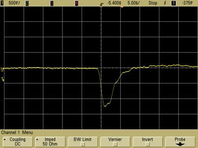
Figures 28 and 29 show the results as displayed on the oscilloscope using the unshielded loop oriented in the both positions parallel to the path over the break in the ground plane, 180 degrees rotated from each other. Both plots have about the same pulse shape, amplitude, and width. Any change between the plots might be attributable capacitive coupling, however the only difference of any note is that the risetime in Figure 25 is a little faster than in Figure 26. The overall difference in the plots is not significant enough to make much difference when using pulse injection for troubleshooting designs.
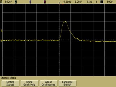
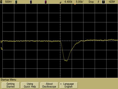
The plots in Figures 30 and 31 for the shielded square loop are also very similar as well as having about the same risetime for both plots. The amplitude of the injected pulse is about 20% less because the distance between the center conductor of the semi-rigid coax forming the loop is further from the path on the circuit board due to the diameter of the coax and the thickness of the plastic housing. The slight improvement in matching of risetimes is not significant enough to warrant the extra complication and cost of shielded loops. In addition, if the scope had greater bandwidth, the resonance at about 600 MHz between the shielded loop and the board would likely cause distortions in the pulses displayed in Figures 30 and 31.
MEASUREMENTS IN THE TIME DOMAIN USING A COMB GENERATOR
(An unusual use for a comb generator)
Possible sensitivity to electric fields/capacitive pickup has been a factor in the past in selecting shielded magnetic loops over unshielded ones. Data is presented to show that in the near field, shielded loops may be required for sensing signal currents in some cases.
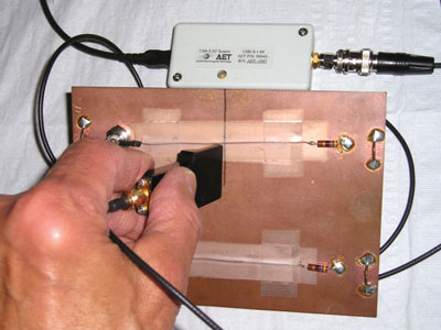
Figure 32 shows a shielded magnetic loop probe held near a ground plane split to sense signal current. Data was also taken using the unshielded wire loop shown in Figure 33 to compare the responses of the two magnetic loops and determine when the wire loop’s electric field sensitivity becomes important.
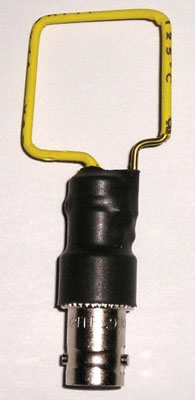
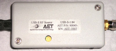
The signal source, shown in Figure 34, for this experiment was an AET USB Powered Comb Generator.[5] Comb generators produce a large number of harmonics that are useful in a number of frequency domain measurements normally made using a spectrum analyzer or similar instrument. But in this case, it was used to furnish fast pulses for the experiment and measurements were made on an oscilloscope. The comb generator used has a 1.8 MHz fundamental frequency and edge rates of about 400 picoseconds.
The output of the comb generator was connected to the BNC connector in the upper left corner of the circuit board in Figure 32. The resulting current in the signal path and the load resistor on the right side of the board resulted in signal current flowing around the split in the ground plane and both shielded and unshieldedloops were used to sense this current.
Figure 36 shows the test setup using the simple wire loop of Figure 33. This is the same setup shown in Figure 32 for the shielded loop except for the use of the unshielded loop.
Figure 37 shows the output of the shielded loop. A resonance at about one GHz can be seen on the waveform. This could be partially due to loop self resonance or capacitive coupling to the shield. To test the effects of electric field coupling, the loop was rotated by 180 degrees. The inductive pickup should invert and any capacitive pickup should stay nearly the same. The reversed loop output is shown in Figure 38 and is just an inverted version of the wave shape in Figure 37. Since the waveforms in Figure 37 and Figure 38 are inverted with otherwise the same shape, capacitive coupling to the loop is not significant for this configuration.
Figures 39 and 40 show the same cases for the unshielded wire loop. One can easily see these waveforms are not just inverted versions of each other. There is significant capacitive coupling between the loop and the circuit made more important by the fast rise time of 400 picoseconds. The capacitive coupling combined with the inductance of the wire probably produced the lower frequency resonance easily seen in Figure 40 and to a lesser extend in Figure 39.
CONCLUSION
The construction details of a square shielded loop were presented along with a source of materials for building one. Square shielded loops are very useful devices.
Parasitic capacitance coupled to a shielded magnetic loop can affect its performance. In this case, a resonance was caused that significantly affected the signal induced into a second shielded magnetic loop.
Frequency response plots of the coupling between small simple wire loops is reasonably flat, similar to shielded loops. This suggests that simple square wire loops may be well suited for injecting signals into circuit boards by inductive coupling.
Capacitive coupling from an unshielded loop is not always a problem that requires the use of shielded loops to solve. On the contrary, sometimes unshielded loops work better than shielded loops. This article has shown that unshielded loops are useful for injecting signals in many cases and into circuit boards specifically. Unshielded loops can even outperform shielded loops in some applications. Given the ease of constructing an unshielded loop and its low cost, this is an important result. Another conclusion that can be drawn is that shields are just thick wires with inductance and capacitance and are not a “magic” solution to prevent unwanted coupling in all cases.
Significant capacitive coupling was demonstrated when using an unshielded wire loop to sense current flowing near a ground plane split. Yet, other results show that for injecting a signal into a signal path crossing a ground break, the simple wire loop was superior. Until more work is done, one must test to see which type of loop works best for a given situation and not just assume that one type of loop is always better.
REFERENCES
1. “Signal and Noise Measurement Techniques Using Magnetic Field Probes,” 1999 IEEE EMC Symposium paper
2. June 2006 Technical Tidbit, “Measuring Structural Resonances”
3. November 2007 Technical Tidbit, Measuring Structural Resonances in the Time Domain – Part 1
4. Missouri University of Science and Technology inductance calculator http://emclab.mst.edu/inductance/rectgl.html
5. AET USB Powered Comb Generator http://www.appliedemtech.com/usbsmain.html
Douglas C. Smith has worked over four decades specializing in high frequency measurements, circuit/system design and verification, switching power supply noise, EMC/ESD, and immunity to transient noise. He has lectured at many universities and delivered public and private seminars. He maintains a website, www.dsmith.org, devoted to high frequency measurements and troubleshooting.
