“Swap-in” connectors can be key in meeting tough emission specifications such as EN 55024 and CISPR 24
Dr. William E. Kunz
Regal Electronics, Inc.
Sunnyvale, California
INTRODUCTION
With clock frequencies of a few hundred megahertz, today’s electronic systems are using pulse edges in the sub-nanosecond range. Networking interfaces deliver data rates approaching 1000 Mbits/s (Gigabit Ethernet and FDDI—fiber distributed data interface) and 155 and 622 Mbits/s (ATM—Asynchronous Transfer Mode). High quality video circuits also use pixel rates in the sub-nanosecond range. These higher processing speeds present never-ending engineering challenges
SOURCES OF RF INTERFERENCE
One such challenge is RF interference, which originates from a fast change in electromagnetic energy. The faster the slew rate (rise/fall times), and the higher the voltage/current amplitude, the more problematic a circuit becomes. As a result, electromagnetic compatibility (EMC) is harder to achieve today than ever before.
While fast changing pulses of current between two nodes of a circuit represent the so-called differential noise source, the fields surrounding this circuit can couple into other components and etch connections. The noise induced via inductive or capacitive coupling represents common-mode interference. The RF interference currents are in phase with each other, and the system can be modeled showing the source, “victim circuits” or “recipients”, and the return path (often the chassis). Several factors are critical in determining the amount of the interference:
- Strength of the source
- Size of the area encircled by the culprit current
- Slew rate of the change
Thus, despite the many possible causes of unwanted interference in a circuit, the noise is almost always the common-mode type. Once there is some RF voltage present between a cable plugged into an I/O (input/output) connector and the enclosure or the ground plane, the resulting RF current of even a few mA can be enough to exceed the allowable emission levels.
TYPICAL CAUSES OF RF INTERFERENCE
Noise Coupling and Dissemination
Common-mode noise can be generated by a less than ideal layout. Some typical causes are an imbalance in the length of the individual conductors in differential pairs, or differences in distance to the power planes or the chassis. Other sources are imperfections in components—magnetic inductors and transformers, capacitors, and active devices such as ASICs (Application Specific Integrated Circuits).
Magnetic components, especially the so-called “slug choke” type storage inductors used in power converters, always produce an electromagnetic field. An air gap in the magnetic circuit is equivalent to a large resistor in a series circuit, where most of the applied power is dissipated. Thus, the slug choke, which is built on a ferrite rod, generates a strong field around the rod, with highest field density near the poles.
In switching power supplies using flyback topology, the transformer must have an air gap, which is associated with the high-density magnetic field. Components that are best suited for “keeping the field to themselves” are toroids, which distribute the field through the length of the core. This characteristic is one of the reasons for the popularity of the toroidal construction in high-frequency networking magnetics.
Circuits with inadequate decoupling often become the source of interference as well. If a circuit requires high pulses of current, and if the local decoupling is not able to support the need because of low capacitance or relatively high internal impedance, the voltage generated by the supply loop drops. This occurrence is equivalent to a ripple, or fast change of the voltage between terminals. Through the stray capacitance of the package, this event can couple into other circuits, causing common-mode problems.
Common-Mode Noise in the I/O Area
When a circuit intended for an I/O interface is contaminated with common-mode noise, the problem has to be resolved before it passes through the connector. Different applications necessitate various ways of dealing with this problem. In video circuits, where I/O signals are single-ended and share the same common return, the solution is to filter out the noise with small LC filters. In lower frequency serial interface networking, some capacitive shunting to the chassis may be sufficient. Differentially driven interfaces, such as Ethernet and FDDI, are normally transformer-coupled to the I/O area, with center taps provided on one or both sides of the transformer. These center taps are connected via high voltage capacitors to the chassis, thus shunting the common-mode noise to the chassis without causing distortion of the signal.
There is no generic solution for all types of I/O interfaces. Designers intent on getting the circuit working often overlook simple details. Some basic rules should be followed to minimize the amount of noise before it reaches the connector:
- Locate decoupling capacitors close to the load
- Minimize the size of the loop of pulsed currents with fast edges
- Keep high-current devices (i.e., drivers and ASICs) away from I/O ports
- Evaluate signal integrity to assure minimum over-or-undershoot, especially in high current critical signals (i.e., clock, bus).
- Use local filtering such as RF ferrites where necessary to absorb RF interference
- Provide a low impedance bond or reference to the chassis in the I/O area
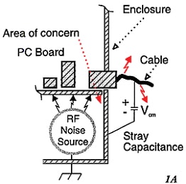
Even if the designer takes most of the precautions listed above to reduce the amount of RF noise in an I/O area, there is no guarantee that the efforts will be successful enough to meet emission requirements. Some of the noise will be conducted, traveling from inside the circuit board as common-mode current. This source of the interference is between the chassis and the circuit-etch of the board. Thus, this RF current will move along a path, through the lowest impedance available, between the chassis and the carrier signal lines. If the connector does not present low enough impedance (bond to the chassis), this RF current will travel via stray capacitance. While it is passing through the cable, the emissions are inevitably generated (Figure 1A).
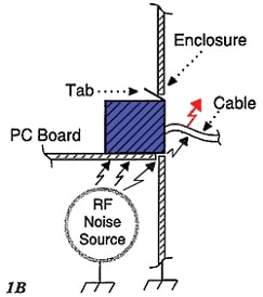
Another mechanism for injecting common-mode currents in an I/O area is through coupling from nearby strong sources of interference. Even some of the “shielded” connectors with a metal cover over the top are not immune in such cases because the culprit source can be located near the bottom of the connector, as in PC environments. If there is an opening between a connector and the reference chassis, the induced RF voltage between these two entities can prove deleterious to EMC performance.
Choosing the Right Connector for Minimizing RF Noise
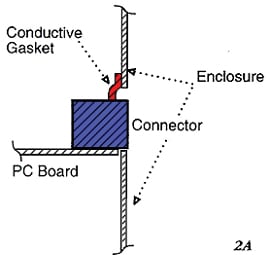
There are techniques for packaging connectors with additional finger stock or gaskets. The connectors provide the bonding by filling the space between the face of the connector and the enclosure. This approach requires gaskets (Figure 2A). Metal or metallic impregnated plastic gaskets work well if they are handled properly—that is, if the surface is free of residue from the installer’s hands, and if the pressure is enough to maintain good, low-impedance contact.
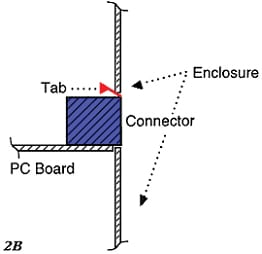
Other connectors are equipped with tabs or another means of making connections to the enclosure. The maximum area of contact in this arrangement is rather small, and optimal contact can be limited by the size of the tab and its flexibility. When using the cutout in the enclosure for a shielded connector, the sides of the cutout must be properly prepared by removing any paint (Figure 2B). Any slack in tolerance may result in this connector being recessed too far inside the enclosure. Also, the bond will become intermittent if the fingers are caught up in any obstacle or are otherwise damaged. Every EMC engineer knows the crucial difference between the “golden system” qualified to meet emission requirements and the one taken at random from the production line in audit. Loose gaskets or bent tabs mounted over paint in critical areas (such as connector cutouts) will cause non-compliance and frustration (Figure 3).

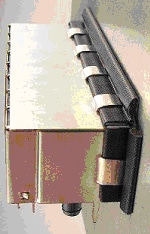
For severe EMI conditions, gasketed connectors should be considered for a number of reasons. Gaskets made of conductive fabric-over-foam are extremely flexible and can be mounted around the whole connector. In PCB mounted applications, a three-sided configuration is usually most appropriate. The mechanical engineer can position the connector within an acceptable through-panel dimensional tolerance of the system package. The connector makes a low impedance bond to the chassis, eliminating concerns over consistency of the contact. A gasket that slides on the inner side of the enclosure wall is much less of a problem vis-à-vis the masking requirements when the paint is applied. For designs with forced cooling, an optimum gasket configuration can provide an additional benefit. In sealing the gap between the connector and the wall, it reduces air leaks. (See Figure 4.) Finally, in a dusty environment, a gasket helps to keep the inside of the system clean.
Compliance Vs. Cost
The total cost of implementing an EMC solution must be considered in the context of the situation, especially if the situation has been brought about by a failure to meet an emission specification such as EN 55024 and CISPR 24. In these kinds of situations, an EMI/RFI problem is typically uncovered by final testing at a testing lab. When designers are faced with options that range from complete circuit redesign to swapping in EMI/RFI suppression connectors in key I/O areas, the swapping option is clearly the more favorable one even though EMI/RFI suppressing connectors are more expensive. It is not unusual, once a connector based solution is identified, to implement a corrective process that is measured in days, as opposed to weeks and months of time-consuming circuit redesign and testing. The key is identifying the “right” EMI/RFI connector, or combination of connectors, that will result in the most cost-effective and timely solution.
Conclusion
Care must be taken to identify and understand the contribution levels and types of interference sources. The variety of connectors available on the market today enables designers to select the optimum design for a specific interface. Standard form-factor RJ-45, mini-din, D-subs and other types of connectors are available fitted with EMI/RFI suppressing shields, filters, or gaskets. “Swap-in” connector solutions might provide the solution to EMI/RFI emission problems that must be solved to meet tough emission specifications such as EN 55024 and CISPR 24.
Dr. William E. Kunz holds a B.S., M.S., and Ph.D. degrees in electrical engineering from the University of Illinois. He has held positions with Watkins-Johnson Company, Mountain Network Solutions, Inc. and WEK Technologies. Dr. Kunz is an executive vice president at Regal Electronics, Inc. (408) 988-2288.

