Tracey Vincent
Application Engineer, CST
ABSTRACT
To attain realistic estimations of simulated insertion loss, all insertion loss components need to be considered and accounted for. In particular, the dielectric and conductor loss components can require careful material parametrization in order for 3D simulated loss to be realistic. An overview of these parametrizations is given, including a focus on the trace cross-section shape influence on conductor loss, an often overlooked phenomenon.
INTRODUCTION
As digital switching times continue to decrease, insertion loss, due to these higher frequencies, increases. The greater loss is caused by several physical properties, categorized by different loss components. Unfortunately it is often the case that one or more of these loss components are not adequately captured during simulation. This often results in a larger than expected measured loss. The loss components, and their physical properties, will be discussed and suitable, full-wave, simulation approaches detailed. 3D, full-wave, solvers are increasingly able to handle more complicated models with better and more detailed parameterization. In addition, certain models with millions of mesh cells can have reasonable run times made available by high performance computing.
There are four distinct high-frequency, GHz range, insertion loss components: radiative, reflected, conductor, and dielectric. Radiative and reflected losses relate to design/topology and are typically, with attention to relevant geometric features, accurately predicted by full-wave electromagnetic solvers. Dielectric and conductor losses depend on material parameters, process parameters, and design/topology. Dielectric loss is the proportion of the signal absorbed by the insulator or dielectric material – the substrate. The conductor loss is the signal that is absorbed by the conductor/metal – the trace; conductor loss can also be known as Ohmic or I²R loss. Dielectric and conductor losses are often inadequately parameterized for full-wave simulations.
The physical mechanism of Dielectric loss and the Dielectric loss parameter, tangent delta, are explored to give a good conceptual understanding of this loss mechanism; guidelines for simulating dielectric material are given.
The circuit topology influences the conductor loss component. Even at DC, the geometry of a conductor or trace determines the overall electrical resistance since resistance relates to length divided by cross-sectional area, the larger this area the smaller the DC resistance. The geometry factor becomes more complicated as frequency increases. At microwave frequencies, the skin effect causes the signal, within the metal trace, to concentrate at the conductor extremities and therefore becomes sensitive to the conductor topography at these extremities. A trace with a sharp edge may have significantly larger conductor loss than a curved edge, however, this phenomena is often not taken into consideration. Examples of traces with different cross section shapes are simulated and their results compared to illustrate this important aspect of conductor loss.
At frequencies at or greater than 10GHz, with materials of high conductivity such as copper, the skin depth is in the order of a micron. At this scale, the shape of the conductor material at the conductor extremities influences the flow of the signal [1,2]. This is considered as surface roughness and is recognized as an important and often underestimated contributor to conductor loss. The influence of surface roughness on conductor loss is mentioned but not explored in depth in this article.
Microelectronics circuits are designed using electromagnetic simulation in order to decrease design costs and shorten the design process. Therefore, circuit design depends on the accuracy of simulation tools that allow circuit prototypes to be created quickly and inexpensively. EM simulation packages, such as CST™, can estimate the total transmission loss if the care is taken with dielectric and conductor loss components.
MATERIAL PARAMETRIZATION
To simplify simulations, and have them run quickly, materials are often characterized into basic materials types such as “Perfect Electrically Conducting” or “Vacuum”. This approach is sufficient for many simulations; however, it can give inadequate estimations of insertion loss, particularly as frequency increases. Understanding the loss components (and their loss mechanisms) and translating that into careful material parameterization and model set up can be crucial for obtaining reasonable simulated insertion loss results.
DIELECTRIC/SUBSTRATE
A dielectric is an electrical insulator that can be polarized by an applied electric field. When a dielectric is placed in an electric field, electric charges do not flow through the material as they do in a conductor, but only slightly shift from their average equilibrium positions causing dielectric polarization. When the value and direction of the field intensity E change, the dielectric polarization also varies in value and direction; during one cycle of an alternating field the polarization is established twice and disappears twice. The dominant polarizing mechanisms at microwave frequencies are electronic and atomic polarization: electronic polarization occurs in neutral atoms when an electric field displaces the nucleus with respect to the electrons that surround it, atomic polarization occurs when adjacent positive and negative ions “stretch” under an applied field. The relaxation time is a measure of the mobility of the dipoles that exist in the material. It is the time required for a displaced system aligned in an electric field to return to 1/e of its random equilibrium value (or the time required for dipoles to become oriented in an electric field). Constant collisions cause internal friction (the physical mechanism of loss in the dielectric material) so that the molecules turn slowly and exponentially approach the polarization orientation with the relaxation time constant. If the relaxation time is many times greater than the period of the alternation of the applied field, polarization is barely able to develop and the dielectric loss is very small. At low frequencies, where the relaxation time is considerably less than the time between peaks, the polarization follows the field and the dielectric loss is also small because the number of re-orientations per unit time is small.
Since the polarization maximum does not occur simultaneously with the maximum of the field intensity, there is a phase shift between field intensity and polarization. Because of this there is also a phase difference between the field intensity and the electrical induction. The electrical induction vector lags behind the electrical field vector by a certain angle, which is known as the dielectric loss angle “tangent delta”. The tangent delta () value is the parameter that represents dielectric loss, it is given as the negative ratio between imaginary, epsilon”, and real part, epsilon’, of the complex permittivity.
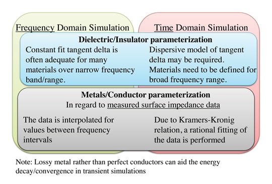
For models that use frequency domain solvers, over a relatively narrow frequency band, the tangent delta value can be parametrized as “constant fit” if the tan delta over that frequency range is known and stable. In reality, no material exists that provides a broadband perfectly-constant tangent delta value. For broadband simulations or transient/time domain solvers (which will use a broad frequency band even if the frequency range if interest is narrow) the tan delta parameter often needs to be better parametrized than constant fit; fast switching certainly involves a broadband spectrum.
For materials that exhibit a single relaxation time constant can be modeled by a 1st order Debye function/dispersion; an example is given by Figure 1.

For materials that exhibit two relaxations, e.g. both electronic and atomic polarization relaxation, a 2nd order Debye dispersion can represent these by the summation of two separate first order dispersions.
If the tan delta of a material has been measured over a frequency range it can be entered as tabulated data, this is a good approach for complex materials such as FR4 [3]. More than one tangent delta value may be defined at different frequency points and the points in between interpolated. FR4 has substantial losses and the loss tangent is quite constant over a wide range of frequencies.
Materials can be complex with different features influencing the fields over different frequency ranges. It is possible to represent tangent delta with the help of other functions such as polynomials.
Conductor/Metals – Surface Impedance Models
Surface impedance parametrization of metal materials relates the tangential electric and magnetic fields on surfaces of the signal trace. The effect of field inside the metal is described by equivalent currents on the surface of the signal trace. Highly conductive metals can be modeled in this way since the E and H fields only penetrate a small distance (the skin depth) inside the conductor. This approach simplifies the model by greatly reducing the number of mesh cells. The surface impedance representation of metals can be used accurately for many models but it does not capture certain geometries such as sharp corners, this is discussed later.
Tabulated surface impedance is given in form of a table with its resistance and reactance tabulated versus frequency. A frequency domain solver computes a linearly interpolated model across the given points. In a time/transient domain solver this table can correspond to “non-physical” or “non-causal” behavior. For example, due to uncertainty or measurement errors, the so called Kramers-Kronig relations could not be fulfilled. Therefore for the time domain simulation a rational fitting of the data will be performed, some material parametrization differences between time domain and frequency domain are given in Figure 2. Tabulated surface impedance can also be generated to reflect the increased impact that surface roughness can impose on conductor loss.
Conductor/Metals – Geometry Influence on Conductor Loss
PCBs/packages are usually fabricated with silver, copper, and sometimes gold because all of these metals are highly conductive. The high conductivity of these materials does result in low conductor loss for the DC-kHz frequency region. At frequencies above the kHz region electromagnetic phenomena induce a skin effect that exacerbates the conductor loss component.
Skin effect is caused by alternating currents inducing magnetic fields internal to the conductor. The internal magnetic field is in addition to the magnetic fields between the signal and ground plane conductors. These internal magnetic fields create induced current loops within the conductor. The current loops produce their own magnetic fields, which oppose the initial magnetic fields; this effectively pushes the current carrying electrons toward the surface of the conductor extremities.
There are many different structures that can be used to transmit high frequency signals. These include: coaxial cable, stripline, and microstrip. These structure have different cross section geometries and therefore, different loss results. In a coax cable topology at frequencies in the GHz region, the skin effect draws the current to the extremities of the center-conductor but since the center conductor is a cylinder, the current density is evenly distributed around the circumference. The stripline structure has the ground plane on both sides of the center conductor/trace. A stripline with rectangular cross-section causes the field, and therefore current density, distribution to be higher at the edges and sides, fig.3. The microstrip structure with its single ground plane causes the fields and current densities to be concentrated on the underside and lower edges of the trace.
The differences in cross-sectional area will lead to differences in conductor loss component. In particular, where the conductor area is limited such as at the corner, the current density increases, this is due to fringing fields [4]. The two current carrying conductors will exert a magnetic force on one another. The magnetic force/field loops around each conductor; therefore the orthogonal electric field is vertical underneath the current strip and horizontal at the edge – known as fringing field. The vertical and horizontal electric fields add; increasing the current density at the edge. It has been noted that a large amount of conductor loss can occur at the edges [5]. The mathematical solution states that current density increases at the conductor edge, becoming larger as the corner gets sharper [6].
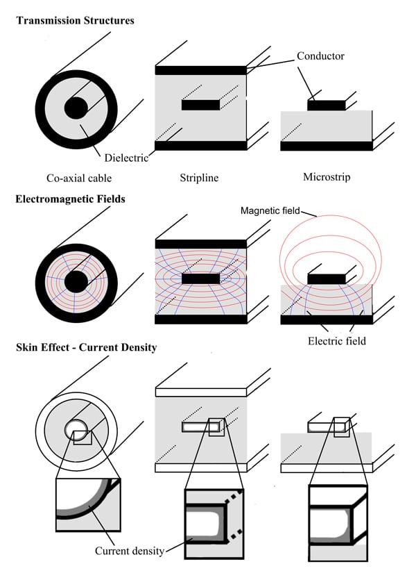
The distributed magnetic and electric fields change as a function of frequency, which changes the current density distribution as a function of frequency. At frequencies close to DC the current density and resistance are evenly distributed across the conductor cross-section geometry. As the frequency increases the current distribution starts to change due to the changing electric and magnetic fields. The current density concentrates at the edges, fig.3; and this effect is often assumed to happen at a medium frequency in the order of 1-5 skin depths of the thickness of the conductor. The medium frequencies are also known as the transition frequency range. At medium and higher frequencies, where the conductor thickness is greater than five skin depths, the current density is assumed to be concentrated at the conductor surface of a skin depth. Both of these maco effects often need to be considered to accurately predict conductor loss[7].
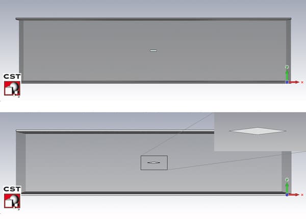
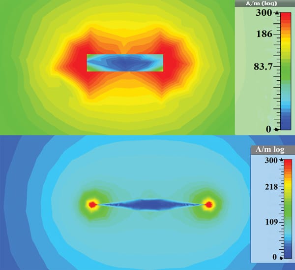
Two stripline traces with the same cross section area, but different cross section shapes, were simulated and found to have significant differences in conductor loss. The stripline circuits have identical parameters: the dielectric is air so that dielectric loss can be neglected, ground-plane silver, they have the same length, and substrate height. One trace has a standard rectangular shape with a width of 0.1mm and height 0.025mm, fig. 4a, this is a common shape used for traces in simulations. The “almond” shape has a width of 0.2mm and height 0.025mm, fig. 4b; therefore, both shapes have a cross section area of 0.0025mm². The almond shape can be more true to some trace shapes for example thick-film print LTCC circuits.
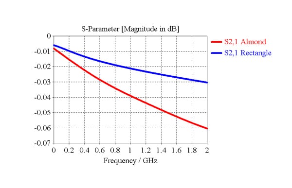
Both stripline models were simulated in CST [8]. The trace was modeled as a normal material with 0.01 mesh cell size, resulting in1.3 million mesh cells for the rectangle trace model and 1.1million mesh cells for the almond trace model. The difference in transmission loss can be seen in fig.5. The rectangular trace has a smaller loss than the almond trace across the frequency band and this difference increases with increasing frequency. These stripline circuits were tested by Lim [9] and the almond trace loss was found to have 130% of the rectangular shape loss at 1GHz.
The H field plots in fig.6a-b, give an idea of the difference in current density between the two trace shapes. For both traces there is a concentration of H-field and therefore current density at the edges. There is a higher concentration of H-field/current density at the edges of the almond trace Figure 6b, compared to the rectangular trace Figure 6a.
Conductor loss is caused by the power dissipated due to the conducting surfaces of the line. The insertion loss of a microstrip line over a low-loss dielectric substrate at microwave frequencies is often dominated by the conductor loss.
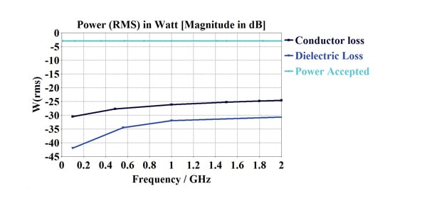
In general, all of these loss components increase with frequency but at different rates. To separate these loss components from measured results is not a straightforward task but straightforward for simulation, fig.7. The losses are for a trace length of 10mm. The conductor loss is larger than the dielectric over this frequency range although the dielectric loss is increasing at a faster rate. The radiative loss component in stripline structures is often small and assumed zero in this case.
With all simulations, certain assumptions are made for each model. Often materials are considered defect free and homogeneous at a maco scale. This is not always the case; further consideration to materials effects can be necessary depending on the material and process.
CONCLUSION
Insertion losses can only be simulated accurately if all the loss components are accounted for. This often includes appropriate parametrization of the dielectric loss component (tangent delta) which depends on knowledge of the material characteristics and finding an adequate model to replicate the characteristic in the numerical computation. Different approaches to replicating the material characteristic are often required for different solver domains.
Signal trace shape can have a large influence over conductor loss and therefore impact total insertion loss. This is illustrated by two traces that have different conductor loss, even though these traces are identical apart from their cross-section shape. Conductor loss is often numerically calculated by a surface impedance method which does not capture geometry effects such as conductor contour/edge.
REFERENCES
[1]S. P. Morgan, “Effects of surface roughness on eddy current losses at microwave frequencies,” J. Applied Physics, vol. 20, Apr. 1949, pp. 352-362.
[2]E. Hammerstad, Ǿ. Jensen “accurate models of computer aided microstrip design” IEEE MTT-S May 1980, pp. 407-409.
[3]A. R. Djordjevic, R. M. Biljic, V. D. Likar-Smiljanic, and T. K. Sarkar “Wideband Frequency-Domain Characterization of FR-4 and Time-Domain Causality” IEEE Transaction on Electromagnetic Compatibility, Vol. 43, No. 4, Nov 2001, pp. 662-667.
[4] J. D. Kraus and D. A. Fleisch, Electromagnetics with applications, 5th Edition McGraw-Hill International Editions, 1999, p 35-115.
[5] E. L. Barsotti, Effect of Strip Edge Shape on Microstrip Conductor Loss, MS Thesis University of Colorado 1990.
[6]J. Meixner “The behavior of electromagnetic fields at edges”, IEEE Trans. Antennas Propagat., vol. AP-20, pp.442 -446 1972.
[7]B. Curran, I. Ndip, S. Guttowski, H. Reichl, “A Methodology for Combined Modeling of Skin, Proximity, Edge, and Surface Roughness Effects,” Microwave Theory and Techniques, IEEE Transactions on , vol.58, no.9, pp.2448-2455, Sept. 2010 doi: 10.1109/TMTT.2010.2058271
[8]CST STUDIO SUITE™, CST AG, Germany, www.cst.com.
[9]M. Lim, J. Wyk “Impact of Conductor Cross-Sectional Shape on Component Performance and Total Losses in a Microsystem” iMAPS/ACerS International Conference and Exhibition on Ceramic Microsystems Technologies (CICMT) 2006.


