Surface current numbers can be used to pinpoint a material with the best absorption characteristics in a given frequency range.
David R. Pacholok, Creative Electronics Consultants, Sleepy Hollow, IL, USA.
With engineers facing ever increasing radiated EMI regulatory compliance concerns, various types of EMI absorber materials have come on the market. These are usually supplied in thin, flexible form with an adhesive back for easy application to a surface within a non-compliant product. Proper material selection is key to achieving EMI/RFI compliance and/or proper system performance.
Most absorber materials for the 10- to 3000-MHz range employ some form of lossy magnetic material such as carbonyl iron or ferrite powder and attenuate the surface currents that unwanted EMI creates when it impacts a conductive wall. These surface currents cause re-radiation of the EM field and often need to be reduced to achieve compliance. They can also interfere with other circuitry, preventing proper system operation.

The comparison of different materials from different manufacturers can be costly and time consuming. With EMI testing labs charging several thousands of dollars per day, trial-and-error testing must be kept to a minimum. Traveling to the EMI lab with a dozen possible absorber materials to see which one works best in the product could prove to be a very costly solution. A simple surface current reduction test fixture (SCRF) is described that allows quick, easy comparison of sample absorber materials and narrows the choices down to the best one or two for a particular problem EMI frequency range.
The SCRF consists of two electrostatically shielded H-field loop antennas that are carefully placed at right angles to each other so that 70dB or better attenuation is achieved over the frequency range of interest. One loop is connected to a swept RF source, and the other to a swept RF receiver. A piece of conductive sheet similar to the product enclosure is placed in a fixed location close to both loop antennas, causing surface current production and re-radiation into the receiving loop. Typically, a 20- to 30-dB rise in received signal occurs. Covering the conductive sheet with a sample of an EMI absorber material causes a measurable reduction in re-radiation. The reduction in re-radiation can be used to compare absorber material performance.
FIXTURE CONSTRUCTION
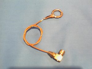
Building a probe as shown in Figure 1 is not difficult. This probe consists of two turns of #24 AWG solid Teflon insulated wire wound on a 1.5-cm mandrel. Larger diameter probes with more turns are more sensitive at the expense of a lower maximum usable frequency.
One end of the loop is soldered to the inner conductor of a coaxial line, and the other end to the shield. Copper tape is used to cover the loop completely, except for a small gap opposite where the coax is attached. If this gap is not provided, the loop is effectively shorted out, is shielded to both H and E fields, and hence is useless. Liberal use of solder connects the tape to the outer conductor and connects each tape wrap to the next. Then, two identical shielded loops must be constructed. The probes pictured in Figure 1 were used from 3.0 to over 600 MHz.

It may be more time/cost effective to order suitable probes from commercial sources. The sampling of manufacturers listed below specify useful frequency ranges for their shielded loops and will serve as a guide.
- ARA Technologies, Deer Park, NY; www.aratech-inc.com
- Com-Power, Lake Forest, CA; www.com-power.com
- Credence Technologies, Soquel, CA; www.credencetech.
com - Electro-Metrics, Johnstown, NY; www.electro-metrics.
com - EMC Test Systems, Cedar Park, TX; www.emctest.com
- Fischer Customer Communications, Torrance, CA; www.
fischercc.com

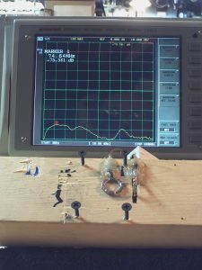
Regardless of the probe “build or buy” choice, the two probes must be carefully aligned at right angles as shown in Figure 2 to achieve minimum coupling. A simple block of wood or plastic makes a convenient support. One probe is connected to a swept RF source; the other to a tracking receiver. While a vector network analyzer was used in our lab, a simple spectrum analyzer/tracking generator combination functions well as long as at least 70 dB of isolation can be achieved between the RF generator and receiver ports. The loops must be mounted on a dielectric fixture such as wood or plastic. The basic fixture can be as simple as a wood block with screws inserted as shown in Figure 2.
The most difficult part of construction is probe alignment for minimum coupling. First, one probe is solidly adhered to the support. The second probe must then be carefully aligned in two dimensions to minimize coupling. A suitable technique is the use of a high temperature, quick-set hot melt glue that is applied only after the approximate probe position is established. Then the probe moved by hand into the precise position to achieve minimum coupling as the glue sets. We were able to achieve 80 dB of isolation over two frequency decades with about one hour of careful trial-and-error tweaking using the hot melt method. The use of one or more clamp-on ferrite beads on the coaxial test fixture cables may be helpful in achieving the needed >70 dB isolation over a wider bandwidth.
The distance between the loops at their closest point is not terribly critical; distances between ½ and 1 loop diameter give good results. Once a loop spacing is chosen and the loops temporarily mounted to provide >70 dB isolation, a metallic sheet of material similar to the intended absorber mounting surface is brought into the proximity of both loops as shown in Figure 3. The best position is the one which gives the highest coupling. An increase of 20 dB or more offers the best accuracy, especially if high absorption materials are tested. A fixture then needs to be built to achieve this same repeatable position during tests.

TESTING
To test a given material, it is attached to the metallic sheet on the SCRF. The reduction in reflected EMI is directly measured by the receiver and is compared with the amplitude of the fixture without the absorber.
While a vector network analyzer is ideal to provide the swept RF source and receiver, a scalar network analyzer that covers the frequency range of interest is also a good solution. Lacking these pieces of test equipment, EMI absorber comparisons can be made with a lower cost spectrum analyzer/tracking generator. All three pieces of equipment will allow swept measurements over the bandwidth of the H-Field loop antennas. If interference is a problem at only a few frequencies, a signal generator and any test receiver can be used if swept equipment is not available.

RESULTS
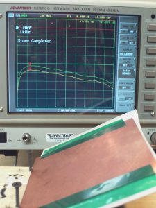
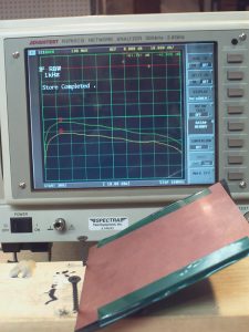
Samples of various EMI absorber materials from Brigitflex Inc.1 and ARC Technologies2 were compared in the surface current reduction fixture. The metallic surface chosen was copper clad FR-4 PCB stock, either single- or double-sided. The size of the PCB stock was three to five loop diameters on each side. The copper side was oriented toward the loops. Figure 4 shows the attenuation of material A in the SCRF, with no absorber present, brought about by the reflection from the copper clad FR-4 surface. The top is the reference trace, while the lower trace shows the added loss due to the absorber under test. Similarly, Figure 5 shows the greater loss of material B under the same test conditions as Figure 4.
CONCLUSION
A simple surface current reduction test fixture was devised to compare the relative absorption characteristics of different EMI absorber materials in a lab environment. While the surface current reduction numbers generated are not absolute measurements of expected EMI reduction, they will quickly point to the material having the best absorption characteristics for the frequency range of interest.
END NOTES
1. Brigitflex Inc., www.brigitflex@foxvalley.net
2. ARC Technologies Inc., www.arc-tech.com
