PCB enclosure design, manufacture and assembly need to be considered early in equipment design to avoid costly modifications and delays in bringing the product to market.
Alan Warner
Tecan Components Ltd.
Weymouth, UK
With the proliferation of electronics, especially wireless and radio applications, in all areas of everyday life, the need for reducing radiated interference between equipment, subassemblies, and individual PCB circuits grows apace. Consequently, shielding and its effect on the manufacturing process must be considered a valid design parameter–one that must be considered on an equal footing with other design goals from the earliest stages of product design. Such a foresighted approach allows designers to sidestep the trap of costly modifications to PCB layouts at the latter stages of the design process. Issues that must be considered include shielding and its effect on the manufacturing process, handling of shielding during PCB assembly, packaging, and the mandated change to non-lead solders.
Preliminary Planning
Is a shield really necessary? At the earliest stages in design, the team should consider that pertinent question. Still, it is generally less costly to provide for an enclosure in the PCB layout, even if one is never used, than it is to attempt to wedge an enclosure into a re-layout after initial testing. This article concentrates on PCB-mounted shielding, the most common form of high volume shielding.
One of the primary issues to be considered at this very early design stage is whether access to the components beneath the shield will be necessary for test, inspection, or rework. Additionally, the method of manufacture and the PCB assembly process itself must be factored into the parameters of enclosure design. Specifically, the enclosure can be designed to meet the requirements of the PCB assembly line, which in the case of high-volume manufacture generally involves machine placement.
Enclosure Design
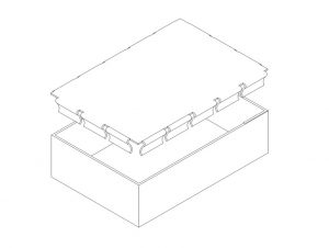
Ready access to the components under the shielding can be achieved by several difference methods, the most common of these being the fence or frame-and-lid set. For the lid, the following options are available, a 3.7mm high spring finger, or a low profile spring finger with a height of 2.2mm as shown in Figure 1. For lower profile components, a pip lock lid is shown in Figure 2.


Other access options include the use of SMT (surface mount technology) clips, available from several sources. In this technique, a five-sided enclosure (four sides plus top) is fitted to an onboard arrangement of these clips after SMT assembly. Alternatively, designers can opt for a five-sided enclosure that features a serrated section around the top of the enclosure that allows most of the top to be peeled back allowing for component access or replacement. Either a lid or metal tape sealed to the largely intact enclosure frame replaces the peeled-off section and restores the enclosure. These designs are referred to as re-work access enclosures (Figure 3).

Machine placement of enclosures generally uses a vacuum pick-and-place head that requires a flat surface target to pick up on–the size of this target is a function of the weight of the enclosure.
Five-sided enclosures, which are to be placed on the PCB at the same time as the components within, will require an array of holes on the surface of the enclosure to allow the re-flow heat to access the components inside. These holes will have some effect on the EMC performance of the enclosure which, if critical, should be measured using development equipment before committing to a final enclosure format.
Enclosure Manufacture
Basically, there are two methods of manufacturing metal shielding enclosures, each with varying advantages and disadvantages.
At the development and low-volume end of the business, one finds photo chemical machining (PCM), a method of creating profiles and detail on thin metal parts. In the case of RFI shielding, these thin metal profiles are generally either hand-formed from bend lines etched into one side of the material or are hard-formed using “V” tools on toggle or fly presses, with each edge formed individually using pre-formatted tooling. Advantages of PCM include the low initial tooling costs and the flexibility of photo tooling. All apertures and other feature are etched at the same time and so the design can be as creative as the designers wish.
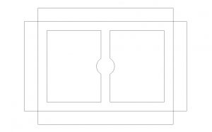
Conversely, there are disadvantages to PCM. First, the cost per item will never be as low as that produced by an alternative method, progression tooling. Also, co-planarity consistency of the shields will never equal that of a progression- tooled product–particularly in the case of low profile fences or five-sided cans. Considering the example of a low-profile fence pinpoints the reason for this shortcoming. Once the profile is etched into the original piece of metal as shown in Figure 4, there is insufficient material remaining for the form tooling to operate efficiently. In contrast, progression tooling calls for the enclosure forming operation to be carried out before the majority of the material is punched out of the item.

A progression tool is a hard punch and press tool involving a number of stages. It takes a continuous strip of metal from a coil; and as the metal progresses through the tool, it forms and punches the detail into the component while it is still tagged (or partially attached) to the strip. The final operation is to break the tags, and the component then leaves the tool ready for use. Because of the size of the tool bed, these tools are usually operated on power presses. The foremost advantage of progression tooling is that once the tool is developed and “hardened,” it will produce millions of components–consistently and at minimal cost. Of course, the main disadvantage is the high cost of the initial tooling, usually thousands of dollars and escalating with every detail of component complexity. Also, the design must be fully “frozen” or finalized to avoid costly modification to the tooling at a latter stage.
Fortunately, there are a couple of halfway stages between PCM and progression tooling that overcome some of the disadvantages of each process. The first is to PCM or laser profile, and then to use one hard tool to form the component. This two-step technique will generally involve one designated hard tool for each component, but at considerably less cost than a more elaborate progression tool. The second is to have two separate hard tools, one to punch the outline and the other to form the component; again each of these tools will be specific to the respective component.
PCB Assembly
The most effective method of fitment of enclosures is to seam-solder the fence or five-sided enclosure directly to the PCB track. This can be a continuous track on the PCB or a series of pads to mate with a castellated enclosure edge. The rule of thumb for the track width is three times the wall material thickness. Using this ratio enables a fillet of solder to form on either side of the enclosure wall, as well as to take up the placement tolerance of the enclosure on the PCB.
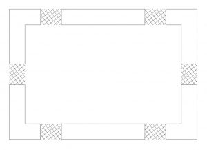
Enclosures, like other large components such as power regulators, require more solder past to be deposited as compared to the amount needed for fine pitch components. This increase can be achieved by using multi-level solder past stencils, the volume of past being a function of the stencil thickness (or depth) as well as the aperture size. For depositing solder past on continuous rectangular footprints, a manufacturer can use a facility known as a lattice stencil (Figure 5). This lattice structure holds the inner portion of the stencil in place while sufficient solder past is channelled via the outer portion of the stencil to achieve a continuous seam around the enclosure edge.

There are two alternatives for the assembly of fence and lid sets. The fence or frame can be placed with the lid fitted at a latter stage in production, usually after automatic inspection or in-circuit testing. Alternatively, the fence and lid can be placed as a set; the lid is removed only if re-work access is required. In addition to the vacuum pick-and-place devices for five-sided enclosures mentioned above, some SMT lines utilize clamp-based pick-and-place machines that grip the enclosures by the side and do not require specific targets. These are generally used for the larger enclosures and may well slow the overall PCB assembly process.
Packaging
If enclosures are to be machine-placed along with other electronic components, they must be packaged in either tape-and-reel or waffle trays. Although tape-and-reel packing is available for enclosures up to 100-mm wide or more, the wide tape will have the effect of slowing down the placement machine as it will take the place of several smaller component feeders. The other alternative, waffle tray packing is not suitable for all placement lines. One advantage of waffle trays is that they are easily re-usable and hence have environmental and cost benefits.
Non-Lead Issue
Traditionally enclosures were manufactured in tin-plated copper, brass, or mild steel; and while these materials in themselves meet the RoHS requirements, the plating will not withstand the temperatures used on non-lead re-flow lines. To overcome this obstacle, there has been a trend toward the use of nickel silver; however, there have been reports, which are still under investigation, of corrosion occurring on the nickel silver parts after re-flow soldering. Although only a very small number of instances have been reported, this problem will require a full investigation before a general switchover takes place.
Conclusion
Although EMC enclosures are not strictly electronic components, their design, manufacture, and assembly onto the PCB needs to be considered at an early stage in equipment design. Such forethought will avoid costly modification and delays in bringing the product to market.
Alan Warner has been the RFI Manager at Tecan for the last seven years and has over 40 years of experience in the electronics industry.This experience includes development of airborne and ship borne military equipment designed to meet the Mil Spec EMC and environmental requirements. Prior to Tecan, Alan was the Test Manager for a medium volume subcontract assembly company with several SMT assembly lines.
