Role of Transmission Lines in High-Speed/RF Devices
In a world full of hype surrounding integrated circuits and chips, it’s easy to overlook another key player in high-speed and radio frequency devices: the transmission line.
Transmission lines are the structures that carry these critical signals between circuits and are commonly found on printed circuit boards via copper traces. They can be thought of as a special highway, guiding these signals from one circuit to another.
On the surface, it might seem like these transmission lines are just copper traces that exist between circuits. While this is partially true, there’s a deeper game at play. As data rates and frequency increase, electromagnetic fields and signal propagation become intertwined.
Transmission lines aren’t just pieces of copper, but carefully designed structures that control how electromagnetic energy propagates. When designed poorly, transmission lines introduce distortion and electromagnetic interference.
The negative side-effects of a poorly designed transmission line can degrade overall system performance which is exactly why engineers invest a lot of time and money into designing and fabricating these structures correctly.
Field Distribution in Microstrip and Stripline
For stripline structures, the line is encapsulated in a uniform dielectric medium sandwiched between two ground planes – forcing the field lines to stay contained inside of the structure.

For microstrip structures, the line rests on top of the dielectric medium and is exposed to air.
Some of the field lines will extend outwards into the air, but also into the dielectric the line is sitting on top of – meaning the fields are only partially contained.
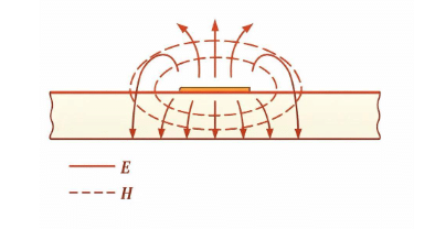
This difference in field containment is what directly drives differences in radiated emissions, susceptibility, crosstalk, and overall electromagnetic compatibility (EMC) performance. This field containment difference is the fundamental reason identical signals can behave drastically differently from an EMC standpoint depending on geometry alone.
Common EMC Misconceptions
The topic of EMC in microstrip and stripline can be a nuanced subject. For example, not all impedance mismatches or discontinuities result in EMC issues.
Theoretically, you would expect a mismatched transmission line (either microstrip or stripline) to leak electromagnetic radiation due to the signal reflecting back towards the source.
In reality, there are a few more factors to consider before taking this assumption as purely factual.
Here are some common EMC misconceptions for radiated emissions, susceptibility, and return path/loop area.
Misconception/Overgeneralization 1:
Reflection = Radiation
Radiated emissions are tied to how well the electromagnetic fields are contained within the transmission line structure.
When a transmission line is uniform, electromagnetic energy remains bound to the structure. Discontinuities along the transmission line can result in signal reflection back to the source.
A common misconception is that impedance mismatches equal radiated emissions. This is not true. Sometimes, the signal is just reflected. You might never realize any radiation.
For example, vias and connector interfaces are common misconceptions of discontinuities that result in radiated emissions due to reflections.
Connector interfaces and vias on a printed circuit board assembly (PCBA) can be well impedance matched up to very high bandwidth. These connector interfaces are thoroughly simulated by connector vendors and are proven to function with low return loss at a specific target impedance (such as 85 Ohm, 90 Ohm, and 100 Ohm differential lines).
Reflections induced by vias and connector interfaces are minimal and will not result in EMC issues if designed properly.
A perfect impedance match is impossible to achieve in practice. There’s always going to be some reflection. In these cases, the reflection is small enough to not be a problem, or it ends up being shielded in some way so that it doesn’t create an emissions failure (such as stripline structures).
Misconception/Overgeneralization 2:
Microstrip = Primary Radiation Contributor
Microstrip geometries are a common trap for overgeneralizations and misconceptions. You would assume that microstrip would be a large contributor to radiated emissions due to the partial field encapsulation.
While yes, the field is exposed to the surrounding environment and does exhibit more field exposure to the outside environment than stripline, microstrip lines can produce radiated emissions depending on the distance to the reference plane.
As the distance to the reference plane decreases, the field lines are tighter and more contained to the transmission line. As the distance increases, the field lines start to spread out.
For example, a microstrip line 4 mils above a reference plane behaves very differently from one 60 mils above a reference plane. Just because the field lines are exposed to air, it doesn’t mean it will automatically produce noticeable radiated emissions.
The same goes for coplanar pours. Fringing fields become less significant when the reference plane is close to the signal traces.
Misconception/Overgeneralization 3:
Coupling Always Happens to Nearby Traces
Engineers often assume if two traces are physically close together, they will couple.
Microstrip and stripline do exhibit fringing fields, but coupling depends on the frequency of the line, the distance from trace to trace, the even-mode impedance (both lines excited in phase), and odd mode impedance (both lines excited 180 degrees out of phase).
Crosstalk exists because the coupled structure supports two different propagation modes. Two traces can be very close together and still exhibit negligible coupling if the geometry and mode behavior don’t support efficient energy transfer.
For example, if the even and odd mode impedances become identical (equivalent), the traces behave as independent transmission lines and energy transfer between them approaches zero. This is given by the coupling coefficient:
Misconception/Overgeneralization 4:
Microstrip is Always More Susceptible to Radiation
Susceptibility is the inverse problem of radiated emissions. Radiated emissions explain which structures radiate, while susceptibility explains which structures are affected by radiation from an external environment.
Which geometries are susceptible to radiation? Susceptibility becomes especially problematic when transmission lines start to unintentionally act as receiving antennas.
This misconception and overgeneralization is the inverse of microstrip being a primary radiation contributor. Microstrip is more susceptible to radiation from the surrounding environment as the line is exposed to air depending on the distance to the signal’s reference plane.
As the distance between the signal trace and the reference plane increases, the fields become less tightly confined. Meaning, the fringing fields can spread further into the surrounding environment which increases the potential for unwanted coupling from radiation in the surrounding environment.
Electrically noisy environments can interact negatively with microstrip structures. The incoming radiation can induce currents and voltages on the transmission line – manifesting in noise or signal distortion.
Misconception/Overgeneralization 5:
Split Planes Always Produce Antennas
In any transmission line, current doesn’t flow in one single conductor, but has to return through a reference conductor. This is typically done by implementing a ground plane and is known as the return path and loop area. Something that could cause unintended EMC emissions would be routing a high frequency line over a split plane.
With a solid reference plane underneath a high frequency signal, the electric and magnetic fields stay tight in between the radio frequency (RF) line and reference plane. When the line doesn’t have the reference plane, the return current can no longer flow beneath the trace and must take a detour around the gap.
The combination of the split plane and diverted return current along the split edge create a slot-like radiating structure antenna. Use copper pours/polygons or solid planes underneath these lines to maintain a consistent reference plane for the current to flow through.
While this is generally good advice, the level of signal degradation and electromagnetic interference (EMI) depends on the gap from one reference plane to another underneath the signal line. The larger the gap, the further the current has to travel to complete the loop.
The issue at heart is how much return current is disrupted. If this gap is incredibly small (maybe 4mils or 5mils), the split plane might not produce a noticeable antenna. It’s not great, but if there are stitching capacitors and vias nearby, the effects could be negligible.
Now, if there was a 500 mil gap for a high-speed clock line, there’s going to be a problem. This is especially apparent in differential lines. The higher the gap, the higher the impedance discontinuity.
To be more specific, single-ended lines produce a larger problem when routed over a split plane since there’s no opposite-polarity trace that suppresses the field. Differential pairs have the opposite-polarity trace, but even with differential pairs, radiation from common-mode noise can increase at the gap.
Keysight ADS General Schematic Used to Model and Simulate a Differential Microstrip Split Plane

Now, should you just go and start routing over split planes even if it’s a small gap? No, you should avoid routing over a split plane, but when designs become dense and real-estate becomes a scarcity, it’s good to know these nuances so you can weigh your options in adding additional layers or other return path/loop area strategies to the design.
Design Tradeoffs
Like many engineering decisions, choosing a microstrip geometry versus a stripline geometry comes down to tradeoffs. It’s also where some misconceptions can arise.
For stripline, there are clear advantages for EMC performance. Radiated emissions and susceptibility remain low as the line is buried in the structure, but the expected tradeoff is cost.
Misconception/Overgeneralization 6:
Avoid Adding Additional Layers to Minimize Cost
Yes, more layers result in higher costs, but this isn’t true for adding two layers to an already existing multi-layer board. A lot of the time, adding 2 layers to a multilayer board is marginal and amortizes to near zero at high volume.
Don’t forgo EMC or compromise routing just to keep manufacturing costs down when adding a few layers will help you pass EMC testing.
Enjoying this article?
Subscribe to Interference Technology for expert coverage of EMI, EMC, and signal integrity challenges—plus immediate access to new digital magazine issues.
Subscribe here →
Misconception 7:
Stripline Costs More Than Microstrip
A common misconception in fabrication is that microstrip structures are less expensive than stripline due to the minimized stackup complexity.
For example, if you have a 6-layer or higher stackup, the cost of etching microstrips and striplines with the same tracewidth is equal. It’s the same imaging and wet process. Just because one geometry is embedded versus one that rests on the surface, doesn’t negate the actual fabrication process of producing bareboard PCBs.
Conclusion
Microstrip and stripline isn’t a black and white subject. There are subtle, but important nuances that guide decision making for creating a successful PCBA with microstrip and stripline geometries. Over the course of this article, seven critical misconceptions were reviewed with the goal of opening the hood to how these structures actually behave.
First, reflections induced from impedance mismatches don’t directly translate to radiated emissions. Sometimes the signal is just reflected. It doesn’t mean the structure will radiate.
Second, microstrip geometries aren’t primary contributors to radiated emissions just because the line is exposed to the surrounding environment. The distance from the line to the reference plane is the bigger contributor. As the distance to the reference plane decreases, the field lines are tighter and more contained to the transmission line. As the distance increases, the field lines start to spread out.
Third, coupling doesn’t occur on microstrip or stripline structures just because two traces are “close together”. Coupling depends on the frequency of the line, the distance from trace to trace, the even-mode impedance (both lines excited in phase), and odd mode impedance (both lines excited 180 degrees out of phase).
Fourth, microstrip is more susceptible to radiation from the surrounding environment as the line is exposed to air, but its susceptibility is primarily dependent on the distance to the signal’s reference plane. As the distance between the signal trace and the reference plane increases, the fields become less tightly confined – making it more susceptible to radiation.
Fifth, split planes don’t automatically always produce antennas. The combination of the split plane and diverted return current along the split edge create a slot-like radiating structure antenna. The level of signal degradation and EMI depends on the gap from one reference plane to another underneath the signal line. The larger the gap, the larger the impedance discontinuity.
Single-ended lines produce a larger problem when routed over a split plane since there’s no opposite-polarity trace that suppresses the field. Differential pairs have the opposite-polarity trace, but even with differential pairs, radiation from common-mode noise can increase at the gap.
Sixth, adding two layers to an existing multilayer board isn’t going to break your budget at high volumes.
Seventh, stripline doesn’t cost more than microstrip. Microstrip and stripline have the same imaging and wet process. Just because stripline is embedded in the PCB doesn’t automatically mean it’ll cost more to manufacture.
This all begs the question, “Why is this subject portrayed in such a black and white fashion and why do these misconceptions exist?” I think there are several reasons:
Reason 1 – Artificial Intelligence
As of late, artificial intelligence posts on popular social media sites have skyrocketed with little to no supervision or correction on material. There’s no editorial board or academic review of these posts. Whether that be for innocent reasons or drawing people towards the paid services they provide, a lot of misinformation can get spread around. Lots of statements can be “true” while also being an overgeneralization.
Reason 2 – Barriers to Entry
The topic of RF, EMI, and signal integrity (SI) is a fundamental intellectual barrier to entry and is safeguarded behind paywalls and academic settings. Courses cost money, simulation programs cost money, and people like to sound smart when discussing a topic not everyone understands right away.
Since the subject is nuanced, how is someone fresh to the field supposed to know what’s fundamentally true or a misconception/overgeneralization without years of research, a pile of money for solid simulations, and training to back up their thought process? Understanding microstrip and stripline structure nuances require a mix of these.
Reason 3 – Mental and Fiscal Investments
It’s easier to read a social media post on the subject than making the mental or fiscal investment into the subject. Even if you did have the training, years of trial and error, and simulations at your fingertips, sometimes it’s easier taking a topic at face value instead of spending the mental bandwidth diving deeper. I myself have fallen into this trap.
Reason 4 – The Intellectual and Surface Level Gap
There aren’t a lot of sources that bridge the gap between intellectually rigorous and handbook/ten-minute-video style language. This is a gap that hasn’t really been explored too much in the topic of RF, EMI, and SI. If you think about it, it’s a fine and very difficult line to dance. How do you explain very technically difficult topics just enough while remaining intuitive and reachable?
Most people either fall into two camps – purely academic or purely surface level. There’s a time for academia and there’s even a time for a quick handbook/ten-minute video, but this uncharted area of blending the two is worth exploring. RF, EMI, and SI is an incredible subject and microstrip and stripline are no exception.
The Takeaway
The goal isn’t to memorize rules like “microstrip radiates” or “split planes create antennas.” The goal is to understand why those statements are often true and where they stop being true.
Good EMC design comes from understanding the underlying physics well enough to recognize the exceptions.