An innovative capacitor design can provide more RFI suppression in a substantially smaller package
Steve Weir and James Muccioli
X2Y Attenuators, LLC
Erie, PA
Instrumentation amplifiers are often employed in hostile noise environments. Sensor lead cables may pick up substantial RF radiation, particularly if they are long and/or not well shielded. When applied to the input of an instrumentation amplifier, RF AC common-mode voltages can result in DC rectification, and a consequential shift in the output operating point of the instrument amplifier.
This article compares a traditional solution vs. a new solution for RFI suppression using a balanced multi-layer ceramic capacitor1 (MLCC) to improve common-mode rejection and prevent DC rectification in instrumentation amplifiers (In-amps).
Traditional Solutions
Traditional common-mode filtering approaches include low pass filters comprised of capacitors and common-mode chokes2. The characteristics of an ideal RFI suppression filter are:
- Inserts no attenuation or phase distortion within the signal pass band.
- Inserts infinite attenuation outside the pass band.
- Is perfectly balanced, which introduces no conversion of common-mode noise to differential signals, or vice-versa.
When using a capacitor, the dielectric material is an important consideration when choosing a RFI filter. For example, microphonic (piezoelectric) effects in X7R type dielectric can cause unwanted signal distortion. To preserve signal fidelity, amplifier manufacturers often specify high quality plastic film capacitors.
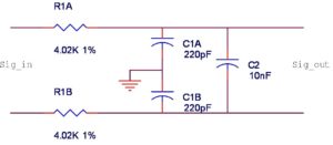
A common starting point is to simply apply a pair of capacitors as low-pass filters; one capacitor to each trace of the differential input. The capacitive filter in each leg rejects RFI above the cut-off frequency (Figure 1).

The common-mode and differential pass band that results is simply:
Fpole_cm = 1/(2* π * R1 * C1).
However, mismatches between the R1A/C1A, and R1B/C1B causes the response near the filter cut-off to be unequal. This mismatch converts a substantial amount of common-mode noise to differential noise. Mode conversion from this filter arrangement can easily reduce the specified 80–140-dB CMRR of a high quality instrumentation amplifier to 30 dB or less. The traditional solution to this problem is to bridge a large value ‘X’ capacitor across the two ‘Y’ capacitors. The large ‘X’ capacitor effectively shorts the sig_out nodes, and thereby equalizes response differences of R1A/C1A and R1B/C1B around the common-mode cut-off frequency (Figures 2 and 3).
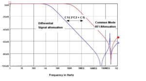
The ‘X’ capacitor shunt has two effects:
- The desired effect of common-mode balancing
- An undesired side effect of differential signal filtering
In order to reduce effects of imbalance, we need C2 >> C1. The differential signal pole appears at:
Fpole_dm = Fpole_cm * C1/((2 * C2) + C1) ≈ C1/(2 * C2)
The greater the mismatch between the two R1X/C1X networks, the greater the required ratio between C2 and C1 and hence the more differential signal bandwidth we surrender in the name of RFI filtering. While resistors with 0.1% or better match are readily obtainable, typically, high quality film capacitors are limited to +/-2% tolerance. Additionally, any mismatches from board layout, manufacturing tolerances, or residue can subvert the value of expensive tight tolerance devices.
Common-Mode Chokes
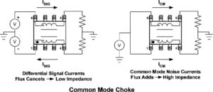
As an alternative to RC low-pass filters, a common-mode choke may be used. In a CM choke based filter, the choke inserts a series inductance in each leg. Coupling between the individual inductors cancels flux from differential currents, and adds flux from common currents. An ideal common-mode choke with perfect matching and coupling between the windings is completely transparent to differential signals, and presents very high impedance to common-mode noise.
The primary advantage of a CM choke is that the signal pass band can extend into the CM reject band. To do so, the source and the load should both be low impedance, such as 50–150-Ohm transmission interfaces. High load impedance loads limit attenuation, as do practical manufacturing tolerances of the choke, and the application PCB. A further problem to watch out for is high Q capacitive loads. The resulting filter can peak strongly around the cut-off frequency, which can result in noise gain (Figure 4).
A Balanced MLCC Solution
An X2Y capacitor is a balanced MLCC solution having three separate electrical pathways within a single device that are attached to four external connections (Figure 5):

The G1 and G2 terminations connect internally to a common reference (shield) electrode within the device, and the A&B plates are separated by the reference electrode. Electrostatically, the three electrical nodes are formed by two capacitive halves that share common G1/G2 reference electrodes all contained in a single ceramic body. The result is a balanced device that offers unique advantages to circuits that require low distortion and high common-mode rejection:
- Both capacitive halves are automatically matched
- Voltage and temperature bias are equalized
- Aging effects on the dielectric are equal
- Dielectric stresses (piezoelectric effects) are opposed within the device.
This unique single component construction facilitates a balanced board layout; Where separate filter devices shunt unwanted currents to PCB board ground using separate paths, the balanced device shunts unwanted currents using a shared path; first to the internal G1/G2 reference electrode, then to PCB circuit ground through the parallel G1/G2 termination connection to a single pad on the board.

The internal plate structure of the balanced MLCC solution forms an Integrated Passive Circuit (IPC) with very interesting magnetic properties. The device structure effectively functions like an autotransformer/common-mode choke. This transformer structure by its geometry dramatically reduces parasitic inductance and is effective into the GHz. The ESR of the multi-layer X2Y capacitor ranges from about 100 milliohms for the smallest capacitors, down to a few milliohms for the larger devices. At frequencies well above the mounted capacitor SRF, inductive impedance dominates. To understand operation, we simplify to neglect the series ESR, and capacitances, and examine the differential and common-mode signal responses:
For A to B difference signals, the autotransformer appears as an inductor with twice the turns as the A ó G1/G2 ‘winding’, and hence four times the inductance. Conversely, for common-mode potentials from A and B to G1/G2 the fields oppose, and the remaining inductance is the difference of the A ó G1/G2 inductance, and coupling factor times the B ó G1/G2 inductance.
Comparing Capacitive Solutions
The inductive coupling in the X2Y capacitor serves to balance the currents in each half of the device and therefore the complex common-mode impedance presented by each filter leg to PCB ground. Combined with the inherent, tightly matched capacitance, the IPC preserves high CMRRs, not only at audio frequencies but up into the low GHz, without a performance compromising ‘X’ capacitor.
For example, consider an instrument amplifier using a traditional 3-capacitor ‘X’ + 2 ‘Y’ filter (Figure 7).


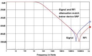
Compared to the same amplifier with a single 10nF rated X2Y capacitor,3 The ‘X’ capacitor in the conventional circuit appears in the differential signal path. For the values shown in Figure 10, differential roll-off begins at 2 kHz, while common-mode filtering does not begin until 40 KHz.
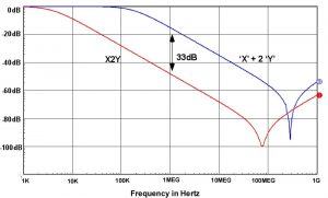
On the other hand, the balanced X2Y circuit contains only two ‘Y’ capacitors. The cut-off frequency for both the common-mode and differential signals is now the same: 4 kHz. Because of the tight balance between capacitor halves, piezo-electric effects are equal and opposite, canceling out. This allows us to use ceramics with the X2Y capacitor yielding little or no signal distortion, where we could not with the traditional discrete filter.
For both circuits, common-mode rejection increases from the common-mode cut-off at 20 dB/decade until the self-resonant frequency of the mounted capacitor is reached. Attenuation then decreases at 20 dB/decade until stabilizing at the ratio of device mounted ESL divided by the combined ESL and the circuit series inductance.
The 2-‘Y’ configuration of the X2Y capacitor exhibits lower effective inductance than conventional capacitors. This affords much greater RFI attenuation than a discrete solution with similar signal bandwidth.
For the circuit response shown in Figure 10 above, the balanced MLCC solution maintains a 33-dB advantage from 100 KHz to over 100 MHz, and a significant advantage at all higher frequencies. In this example the X2Y capacitor signal bandwidth is 4 kHz versus 2 kHz for the conventional configuration. Setting the device’s signal bandwidth to 2 kHz would increase the insertion loss advantage of the X2Y to 39 dB+.

Test Results
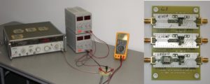
Test circuits were constructed using the:
- Traditional ‘X’ + 2 ‘Y’ capacitor configuration shown in Figure 7.
- Common-mode choke solution shown in Figure 4.
- Balanced MLCC filter shown in Figure 5.
The inputs were shorted together with a 50-Ohm shunt to ground and driven with a 1 V p-p, 1 KHz to 10 MHz sweep signal as measured at the input shunt.
All three filters performed as expected, suppressing RFI rectification that would be visible as a shift in the DC output. Both capacitive circuit solutions exhibited very good common-mode rejection.
Conclusions
The novel construction and equivalent circuit of the balanced MLCC is uniquely suited to RFI suppression applications:
- Compared to the traditional ‘X’ + 2 ‘Y’ filter, a single balanced MLCC simplified the filter circuit, using significantly less space on the printed circuit board to achieve the same result as three plastic film capacitors.
- Compared to the common-mode choke solution, this device provided significantly more RFI suppression in a substantially smaller package.
- The X2Y capacitor uses standard X7R dielectric instead of specialized film dielectric to provide cost effective RFI suppression in a dramatically smaller package than both traditional filter solutions tested.
Only X2Y capacitors have the combined features—tightly matched capacitors and integrated GHz common-mode magnetics. In addition to use as RFI input filters, the amplifier circuit was further improved by substituting one X2Y capacitor in place of the four conventional capacitors used for power bypassing, allowing for further simplification, size reduction and cost savings.
Endnotes
- X2Y® Capacitor, www.x2y.com
- Kitchin, Charles and Lew Counts. A Designer’s Guide to Instrumentation Amplifiers, 3rd Ed., “Designing Practical RFI Filters” pp 5-12 and “Using Common-Mode RF Chokes for In-Amp RFI Filters” pp 5-20. Analog Devices, 2006.
- Common-Mode Filters Using X2Y® Capacitors, pp 5-19
Steve Weir, Member Technical Staff, X2Y Attenuators, LLC is an independent consultant with over 20 years ‘plus industry experience with a broad range of circuit design expertise. Steve holds 17 U.S. patents, and has architected a number of TDM and packet based switching products, consults on patents and is a frequent contributor to the SI-list signal integrity reflector. Email: sweir@x2y.com.
James Muccioli, Chief Technology Officer, X2Y Attenuators, LLC has over twenty years of EMC experience, both with DaimlerChrysler and United Technologies and is inventor or co-inventor of 19 Patents while at DaimlerChrysler. Jim has extensive experience in EMC design, analysis, testing, and is an active member of SAE J-1113/J-551 EMC committees. Jim is a NARTE certified EMC and ESD engineer. Email: james@x2y.com.
