Currently, there is an ongoing discussion among SI and EMC engineers on the fine points of PC board design for best signal integrity and EMI performance. Among the topics it seems designing in gaps or slits in ground return planes always comes up.
Gaps can also occur mistakenly due to the addition of some connectors or other object that creates gaps in the copper. In fact, one of the first things I look for during design reviews is to inspect the ground return planes for inadvertent gaps. This is such an important concept when designing PC boards that I recorded a short video demonstration showing the EMI consequences.
Of course, there are valid reasons for partitioning the return (and/or power) plane in cases where digital and sensitive analog circuits need to be isolated. But for most cases a solid return plane is a better practice. The problem occurs when a high frequency clock trace or other fast digital signal crosses one of these gaps. There are numerous other papers on this issue (refer to the References at the end for more information). In this posting, I’d like to illustrate why it’s bad from an EMI viewpoint.
Besides the obvious reflections noted by both Smith and Bogatin, there is also a differential to common “mode conversion” that occurs, which causes two bad things:
- Common-mode currents are generated, which create harmonic noise currents, leading to board and cable resonance and related radiated emissions.
- The gap forces the electromagnetic field normally confined in the dielectric between the clock trace and underlying return plane to “wrap around” the entire PC board, coupling to other nearby traces and causing cross-coupled noise (or crosstalk).
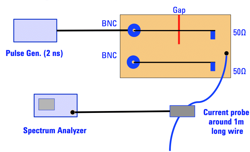
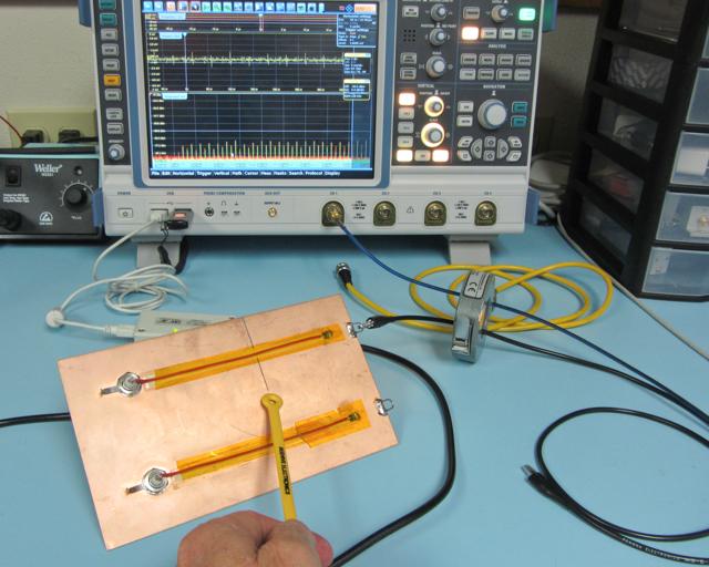
A simple experiment was set up based on the experimental PC board Smith devised. The board consists of two wires taped down to a copper clad board. These represent (near 50 ohm) circuit traces, one end of which is terminated to a 49.9-Ohm resistive load and the other end connected to the center pin of a BNC connector attached to the board. One trace has a 4 cm gap in the return plane – the other trace has a solid return path (Figure 1).

The experiment consists of three parts:
- Tracing and observing the path of the electromagnetic wave in the return path (both gapped and untapped traces).
- Observing crosstalk in the non-driven trace when the gapped
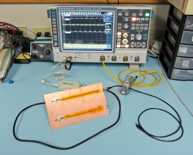
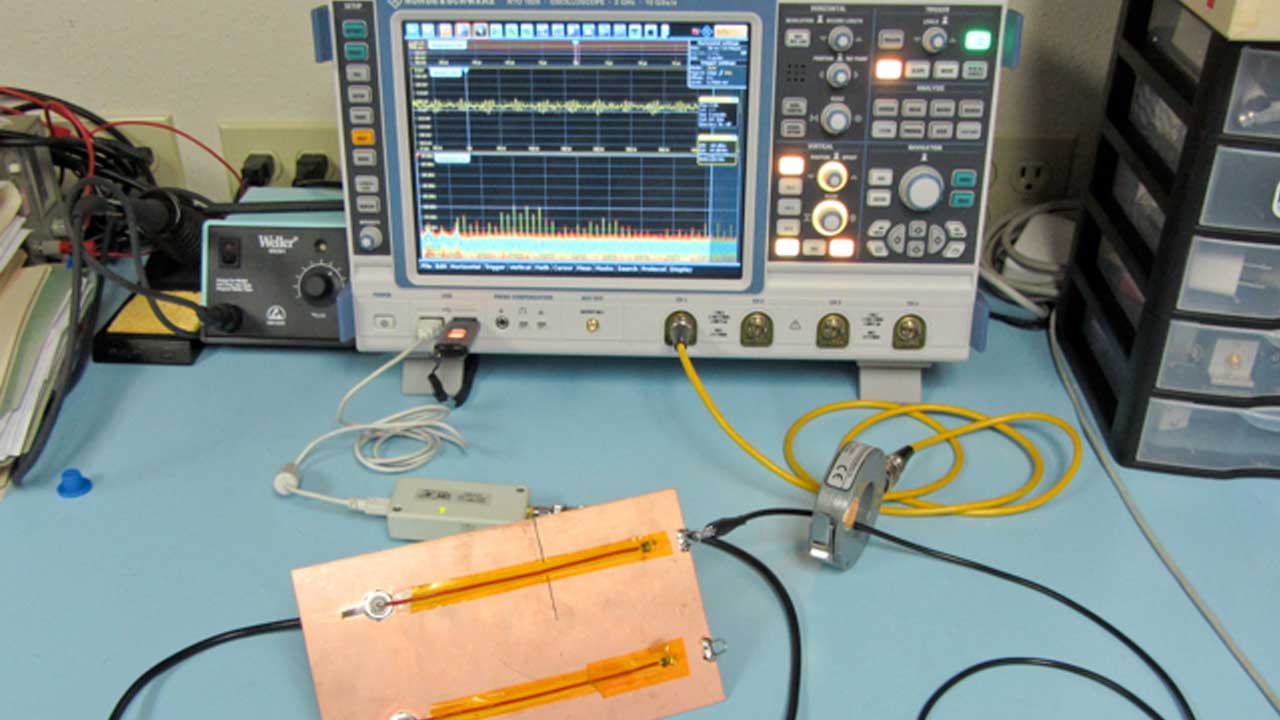
- Observing harmonic currents in a clip lead (simulating an I/O cable) attached to the board plane when the gapped trace is driven.
The board is driven with a USB-powered harmonic comb generator from Applied Electromagnetic Technology (AET), which is essentially a fast-edged pulse generator. The pulse generator is connected to each BNC connector in turn and an Beehive Electronics H-field probe is used to trace the path of HF current.


In summary, routing high speed fast-edged traces over gaps in return planes causes both radiated emissions and cross-coupled noise. If gaps must be used the return path can be controlled by adding stitching capacitors across the gap and near the high speed trace (really best added on both sides of the trace). I recently produced a short video demonstrating the effects noted above. The experiment is easily set up if you’d like to duplicate it for your colleagues.
References:
- Doug Smith, Crossing the River: The hazards of crossing a split-plane gap with a high speed signal, 2008.
- André and Wyatt, EMI Troubleshooting Cookbook for Product Designers, SciTech Publishing, 2014, page 31.


