INTRODUCTION
We often design electronic products only to find that when we test them for electromagnetic compatibility (EMC), their emissions and/or immunity are not as good as we need them to be.
Usually, at this time, we feel as if we are fighting against the laws of physics to contain the conducted and radiated emissions, or to reduce susceptibility.
But in fact the laws of physics – Maxwell’s Equations – are causing our design to have the best emissions and immunity that the physical structure allows. We might say that our product is doing the very best it can to reduce its emissions and improve its immunity!
(I am using the word “product” to mean every type of electronic assembly, from modules, subsystems, equipment and systems, to installations.)
The key issue – is that all currents (including strays) always flow in closed loops, and always take the path of least impedance, whether this path is along conductors or through the air (or other dielectrics) between them.
Current flows in the path of least impedance to minimize the energy in its associated electric and magnetic fields, rather like the way a drop of water in air assumes a globular shape to minimize the energy in its surface tension.
Because currents naturally take the paths that result in the lowest EM field energies, they automatically give us the best emissions and immunity of which our design is capable. Rather than fighting the laws of physics, what we are fighting is our own lack of understanding of how the laws of physics work. Once we understand this we can work with these laws from the start of our design, to easily and quickly create cost-effective products that meet their EMC specifications.
Unfortunately, the way that Maxwell’s Equations are taught doesn’t show how easy it is to derive (without any mathematics!) the easiest, simplest, most profitable way to design products using good EMC engineering techniques [1].
Signal Integrity (SI) and Power Integrity (PI) are subsets of EMC engineering, so employing good EMC design techniques from the start of a new project ensures excellent SI and PI (see [2]).
This has the effect of considerably reducing the number of design iterations, generally reducing overall cost of manufacture, and reducing time-to-market.
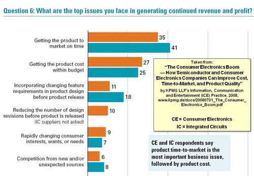
Time-to-market has, since 2000, become the most important issue for a financially successful electronic product. This is shown by the industry responses to Question 6 in [3], see Figure 1, and I have seen other reports from similar prestigious organizations that show the same for most electronic applications.
It is often found in practice that employing good EMC design techniques from the start of a project improves functional performance, sometimes even giving signal quality and functional specifications better than anything that had ever been achieved before.
Unfortunately, some project/engineering managers insist on the lowest Bill Of Materials (BOM) cost, believing that this will somehow lead to the most profitable product.
Where it prevents us from working with the laws of physics, we often find ourselves fighting this ill-advised and plainly incorrect approach (see [4]). The result is a number of additional delays and cost-increases (e.g. adding filtering and shielding to pass EMC tests) that increase the overall cost-of-manufacture, delay market introduction, reduce profitability and increase financial risks.
For example, the ideal printed circuit board (PCB) layer stack for good EMC design of a given product might have eight layers, but the minimum SI and functional specifications can be met with just six. The cost-saving achieved by using the six-layer board is considerably outweighed by the extra delay and cost of adding filtering and shielding at the end of the project to meet its EMC specifications.
The overall cost of manufacture ends up being much higher than would have been achieved with an eight-layer PCB, and the (more important) time-to-market is delayed by several weeks – which in some situations can make the difference between a product’s success and its failure.
This article briefly introduces the laws of physics as they apply to our products’ SI, PI and EMC design issues, developing an “EM Design Toolkit”. It then briefly describes applying that toolkit to a PCB assembly example.
I wrote a similar type of article on applying these same laws of physics to ease the EMC design of systems and installations or any size, [5], which might be of interest to some readers.
EXTERNAL AND INTERNAL EMC
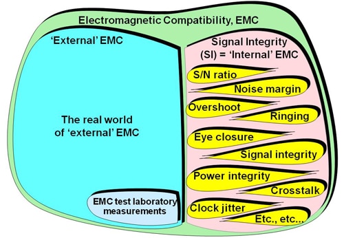
Apart from DC issues such as the fan-out of DC signals or the voltage drop caused by resistance in DC power conductors, all SI and PI issues are just subsets of EMC, as Figure 2 tries to show (also see [2]). They might be called “internal EMC” – the product interfering with itself. For more detail on this, see Chapter 8 of [6] or 2.10 of [7].
EVERYTHING HAS PERMEABILITY (µ) AND PERMITTIVITY (ε)
All media and materials in this universe have conductivity, permeability (µ) and permittivity (ε).
In vacuum (and air):
µ0 = 4π10-7 Henries/meter
ε0 = (1/ 36π10-9) Farads/meter
Other media and materials are characterized by their relative permeability (µR) and permittivity (εR) – dimensionless numbers, just multipliers for the vacuum permeability and permittivity – so their overall permeability is: µ0µR and their overall permittivity is: ε0εR
Permeability is associated with inductive EM energy, which we draw as magnetic field contour lines.
Permittivity is associated with capacitive EM energy, which we draw as electric field contour lines.
Conductivity (and its reciprocal, resistivity) is associated with energy loss, i.e. the conversion of EM energy (magnetic or electric) into thermal energy.
The shape and size of conductive structures carrying current, and the µ0µR and ε0εR of the media or materials they are embedded in, cause inductance (L) and capacitance (C), respectively.
This means that whenever there is a fluctuating voltage (V) there is always an associated current (I).
And vice-versa: whenever there is a fluctuating current (I) there is always an associated voltage (V).
Some digital designers assume that because the input resistance of a CMOS gate is several MΩ, PCB traces carrying digital signal voltages carry no (or a very tiny) current. This is incorrect because it ignores the inevitable (and unavoidable) stray capacitance of the traces and the gate input.
For example, with a gate input capacitance of 3pF and a 3 Volt digital signal rise-time of 300ps (quite slow these days) the peak current required just to charge up this single input gate alone is about 30mA. This intense current “spike” must flow in a loop that includes the DC power supply distribution network, so can cause all manner of SI, PI and EMC problems.
In insulators and dielectrics (e.g. air, PVC, fiberglass) µ0µR and ε0εR cause analogous effects to inductance and capacitance – so whenever there is a fluctuating electric field (E) there is always an associated magnetic field (H).
And vice-versa: whenever there is a fluctuating magnetic field (H) there is always an associated electric field (E).
Chapter 2 of [6] and 2.3 of [7] have more details on the above.
BECAUSE OF MAXWELL’S EQUATIONS…
Every fluctuating voltage or current is really EM power (Watts, i.e. rate of flow of electrical energy), propagating as a wave in the medium with velocity v = 1/√(µ0µRε0εR) m/s (≅ 3.108 m/s in air or vacuum) and creating electromagnetic (EM) fields as it does so.
This applies to every kind of electrical event, whether we call it electrical power; electronic or radio signals; infra-red; light; lightning, etc., and including all mains 60Hz power; analogue, digital and switch-mode power and signals; data communications; radio-frequencies (RF) and microwaves, etc., including all electrical, electronic, or radio “noises”.
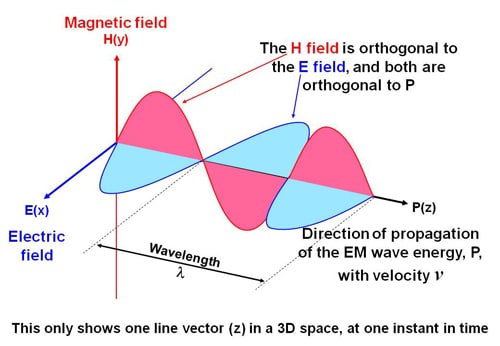
Figure 3 is an attempt at visualizing a single vector of an EM wave at a single frequency, as it propagates in free space. Its shows that the E and H fields are perpendicular to each other, and that they both fluctuate in directions perpendicular to the direction in which the EM power is propagating.
The usual analogy is with waves on the ocean, which propagate wave energy across the surface of the ocean even though the molecules of seawater in a wave only move up and down.
A common way of visualizing the E and H fields associated with voltages and currents in conductors, is shown in Figure 4, for a send/return pair of conductors shown in cross section. E-field lines always terminate on conductors, perpendicular to their surface, and H-field lines never terminate on anything.
These lines should be considered like contour lines on a geographical map – they are not real, but their density (number of lines per inch) indicates the strength of the field (like the slope of a hill). So we can see that the E and H field strengths are highest in between the send and return conductors.
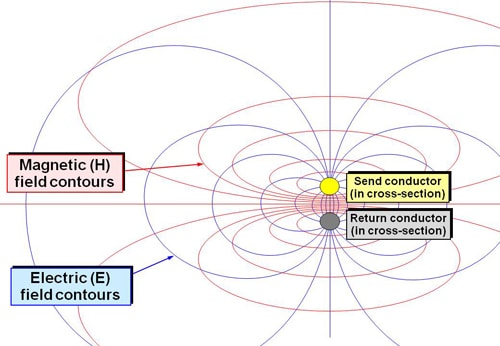
The electrical power associated with the current in the wires propagates along the length of the wires. Because Figure 4 shows the wires in cross section, the electrical power (i.e. propagating EM energy) is flowing perpendicular to the surface of the page or screen with which you are reading these words, and the E and H fields it sketches are fluctuating in the plane of the paper or screen.
Maxwell’s famous four equations include Amperes Law, which says that currents always flow in closed loops, and Faraday’s Law of electromagnetic induction, which says that currents always flow in such a way as to minimize their loop areas.
Maxwell himself invented the concept of displacement current, showing how a fluctuating current could flow through capacitance even though there was no conductive path for it.
BECAUSE OF THE LAW OF CONSERVATION OF ENERGY…
Ignoring the virtual particles in the “quantum vacuum”, [8], there is always zero EM power at any point in space. The EM power entering a point must be exactly balanced by the EM power leaving it.
This is Kirchoff’s current law, which is often described as: “the sum of the currents at any point equals zero”, and is equivalent to Ampere’s Law.
Another way of putting this is to say that all currents flow in closed loops. If some current could escape from a loop and go wandering off on its own, never to return, then at the point where it left the main loop there would be an imbalance in the current. Current would accumulate at that point, and the Law of Conservation of Energy tells us this can’t happen (in our universe, anyway).
So we see that Conservation of Energy (in this context sometimes called the Law of Conservation of Charge) means we could rewrite Kirchoff’s current law as: “the sum of the EM power at any point equals zero”.
This means that at any circuit node that sends a current (whether power, signals, noise, etc.) also simultaneously emits an antiphase current that we call the return current.
These send and return currents propagate through the impedances of the various media (air, conductors, etc.), eventually meeting up to create what we think of as send/return current loops. At any instant in time, the currents in the send and return current paths balance each other out.
Notice that because all power, signal and (stray) noise currents, of any kind, flow in closed loops, this means that the connection to the safety earth/ground electrodes generally has no relevance at all for good SI, PI or EMC design.
(In poor EMC designs, stray current loops can travel through the safety earth/ground, using it as a convenient conductive structure, and causing high levels of emissions and poor immunity.)
BUT IT’S REALLY ALL BECAUSE OF QUANTUM ELECTRODYNAMICS (QED)
How did the return currents “know” what paths to follow to exactly match up with their respective send currents? Prof Feynman’s slim book, [9], says that propagating EM energy (light is also EM energy) takes the path of least time – which is also the path of least energy – which is also the path that gives the best SI, PI and EMC possible for a given geometry and media/materials (although this last conclusion is not found in [9]).
To find out how propagating EM energy “knows” to do this, we have to integrate over the whole of space and time, including negative time. This was Prof Feynman’s great insight, which made the world of quantum electrodynamics amenable to calculation, and is responsible for much of modern electronic technologies.
But when Prof Feynman’s students asked him what underpinned this natural behavior, he said no one knew and there was simply no point in even asking the question. It was just the way nature worked. However, some progress is now being made in answering this question, with the favored solutions being the “many worlds” or “parallel universes” theory, which is known to be true because otherwise quantum computers wouldn’t work.
A characteristic of QED is that it defies common sense and destroys the time relationship between cause and effect, with some outcomes that can seem very weird. Apparently, with sensitive enough instruments listeners could hear what the outcome of a ball game would be by listening to radio broadcasts from the future! Unfortunately it only reaches a few femtoseconds into the future – not enough time to place a winning bet.
Also, QED permits the power budget for a point to deviate from zero for a few femtoseconds, but after that the Law of Conservation of Energy insists that the power books have to balance to zero once again, as described in 5 above.
Maxwell’s Equations and related laws of physics describe a common-sense, cause-and-effect world in which understanding basic concepts makes it quite easy and quick to design low-overall-cost good SI, PI and EMC – but the QED concepts that underpin this are very weird and wonderful.
Despite its weirdness, QED is the most well-proven theory ever known, and has been proven to be accurate to about 11 orders of magnitude more than has (so far) been possible for gravity.
Happily, for all SI, PI and EMC work, engineers need go no deeper than Maxwell’s Equations and Conservation of Energy (or Charge).
WHAT DOES ALL THE ABOVE MEAN FOR SI, PI AND EMC?
EM Power Divides Between Alternate Paths According to Their Admittances
In the “far field” of an EM source, E and H fields experience the “wave impedance” of the media or materials their EM power is propagating through:
in air or vacuum: √(μ0/ε0)=120πΩ (near enough 377Ω)
in other media (e.g. PVC, oil, fiberglass, etc.):
120π√(μR/εR)Ω
These simple wave impedance formulae are only true in the “far field”, typical for radio transmission and reception, whereas in the “near field” the impedance situation is more complex, and the dominant effects on the impedance of a path through the air or other dielectric are inductive and capacitive coupling – often called “stray” or “parasitic” inductance and capacitance. See Chapter 2.4 of [6] or 2.3.3 of [7], for more on this, including how to calculate whether we are in the near or far field.
For EM waves propagating along conductive structures (what we call power, signals or stray currents flowing in cables and PCB traces), the medium surrounding them has an important effect on impedance, but so does the shape of the structures carrying the current and the shape and proximity of nearby conductors – most especially the return conductor(s), but any other conductors in the near field will also have an effect.
So EM waves propagating along conductors can experience impedances that are lower, or higher, than the impedance of the medium surrounding them.
This means that for a fluctuating current travelling along a conductor there are always alternative paths in the air and other dielectrics, so its send/return current loop is never a simple one.
In fact, all currents always split and flow in multiple alternative paths, in proportions according to the admittances of each of the paths (a path’s admittance is the reciprocal of its impedance).
This is conceptually no different from the way that a DC current flowing through a bunch of parallel resistors will divide up according to their various conductances (reciprocal of their resistances) – with the highest current flowing in the resistance with the lowest value (i.e. the highest conductance).
The big difference for fluctuating currents is what is sometimes called “the invisible schematic” – the impedances of the stray capacitances and inductances, which are alternative paths for EM energy to flow in, which successful practical EMC engineers learn to visualize whenever they look at conductive structures.
Each part of a current loop has several alternative paths. The paths can be along conductors or through components and devices, or through the stray paths in the insulation, PCB substrate, air, etc.
It simply doesn’t matter to a propagating EM wave. The conductors, components and devices that we designed, and the stray capacitive/inductive coupling and “accidental antenna” emissions (see 7.2) that we didn’t design and not wanted (but can’t be prevented entirely) all just look like different admittances (reciprocals of their impedances).
For example, a significant portion of the EM wave power might leave a conductor and continue on its path by travelling through the air – for example as a (capacitive, E-field) displacement current – if it sees that air path as having impedance comparable with that of the conductor.
When a conductor resonates (i.e. is not a well-matched-impedance transmission line, see 7.6) in a way that creates a high impedance, a “stray capacitance” path through the air can easily create a lower loop impedance, causing most of the current to travel as displacement currents.
And where an air path resonates in a way that creates a low impedance, it could easily create a path with much less loop impedance than that of the intended conductors, so once again most of the current can travel as E-field displacement currents in the air.
We could say that our main task of SI, PI and/or EMC designers is to reduce the proportion of the EM waves (wanted currents) that “leak out” of our conductors – “escaping” into nearby conductors via stray capacitance and inductance (what we call crosstalk), and also “escaping” into the air as far-field EM waves (what we call EM emissions and measured with antennas in test labs).
It is important to understand that every current loop, however formed, with however many branching current paths going wherever, always has to return exactly 100% of the EM energy back to its source, to comply with the law of conservation of energy.
Actually, the reality of power and signal propagation is not that a current starts off from a voltage source and eventually returns back to it – having flowed around a loop or loops – but that the send and return currents are actually generated simultaneously by the source, and balance each other out at every instant thereafter.
Anyway, this perspective that current flows in multiple paths according to their admittances, shows that – to achieve good SI, PI and/or EMC – all we need to do is control the impedances in the various paths that are available to our wanted signals or power currents, so that they travel predominantly in the loops we want them to.
For example, if it was possible to design so that no signal or power current was “lost” to alternative paths, then we must have no crosstalk, no emissions, and – as a direct result – our product’s SI and PI must be perfect and its EM emissions zero (see [2]). Also, by the Principle of Reciprocity (see 7.2 below), its RF immunity would be perfect.
Of course, perfection is never achieved but we can get close enough to reduce emissions to sufficiently small amounts, and improve immunity by as much as is needed, without adding significantly to the overall cost of manufacture, simply by working with the laws of physics.
For more detail on this topic, see Chapter 2 of [6], 2.3 of [7] or 10.1.4 in [10].
All Conductors are “Accidental Antennas”
A transmitting antenna is merely a conductor that intentionally leaks its voltages and currents as EM power into the air. A receiving antenna is simply a conductor that intentionally picks up voltages and currents from the EM fields around it.
Of course, the more usual situation is that we don’t want our conductors to transmit (leak) some of their EM power, or pick up noise from the environment. EMC engineers usually call the fact that they always do leak and pick-up: “accidental antenna behavior” or “unintentional antenna behavior”.
When a conductor is exposed to E, H or EM waves propagating in its insulating medium (e.g. the air), its electrical/electronic circuit experiences the same voltage and current noise that we would need to create if we wanted to generate the exact same field pattern at the conductors. This is called the Principle of Reciprocity.
The Principle of Reciprocity also applies to accidental antennas, so when a conductor carrying a current has imperfect control of the wanted current loop that results in noise emissions, it will suffer noise pick-up from its EM environment in exactly the same way.
When electronic engineers are discussing SI or PI, they usually call accidental antenna behavior crosstalk, and they notice that the same techniques that reduce the noise coupled from the crosstalk’s “aggressor” or source also help reduce the noise picked up by the crosstalk’s “victim” – another example of the Principle of Reciprocity.
Current Loop Size and Coupling
The transfer of EM power from one conductive circuit to another – whether intentional or not – is called EM coupling. It can be described by “coupling coefficients” which are (of course) frequency dependent because they represent stray capacitance and inductance.
Up to the first resonant frequency, the larger the area of the send/return current path’s total loop, the larger its impedance, the smaller its admittance, and the larger its E and H field patterns and hence its coupling with other conductors.
As shown in Figures 5 for E-fields and Figure 6 for H-fields (and Figure 10, see later) the larger the current loop, the higher is the proportion of its wanted current that couples with (leaks into) “victim” circuits, causing higher levels of noise currents flowing in unwanted loops, increasing the waveform distortion in wanted signals, and worsening emissions and immunity.
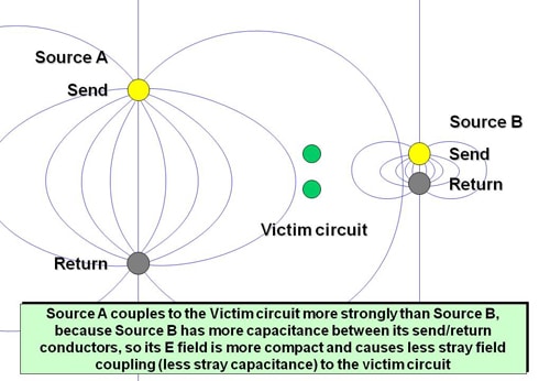
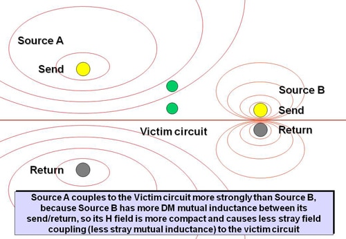
Figures 5 and 6 show us that it is important to minimize the send/return current loop areas, for all circuits – whether they are accidental transmitters or receivers of EM noise – to maximize their SI, PI and EMC. For more detail on this, see Chapter 5 of [6], 2.7 of [7] or 10.1 of [10].
All Currents (Including Strays) Naturally Take the Path of Least Impedance
The fact that currents naturally “prefer” to flow in the path with the smallest loop area and lowest impedance (described in 6 above) is the only way that I know of where the laws of physics work with SI, PI and EMC designers, instead of against us.
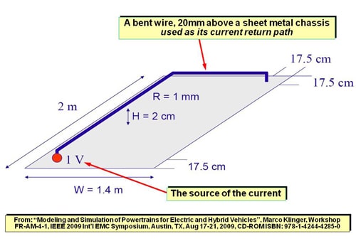
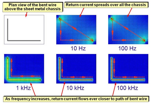
Computer field solvers show this phenomenon very clearly. Figures 7 and 8 are copied from [11], and show that when a bent wire carrying a current is routed close to a sheet metal chassis that it is using as a return path, the return current flows almost exclusively in the metal that lies underneath the wire, following its bent path, at frequencies above about 1kHz.
This is because the return path in the metal sheet below the bent wire creates the current loop area with the lowest possible overall impedance for that structure, even though the return current has to go around a bend to achieve it.
The red dotted lines in Figure 8 were drawn by the authors of [11] to help readers understand where the mean or average current return paths lie, because the EM field solver simply provides color gradients.
Notice that above 1kHz, although the return current is flowing in part of the metal sheet, the rest of the sheet is “quiet” – i.e. it has no currents flowing in it and so no voltage drops across it.
Circuits using those quiet parts of the sheet for their current return paths (e.g. as their 0V plane) do not suffer any voltage noises from the bent wire’s return currents. (At 100Hz and below the impedance of the sheet is so low that the voltage noise caused in the other circuits by the now-widely-spreading return current are generally negligible).
This is a very important result that shows that we can have many different segregated areas of circuits (e.g. digital, analogue, switch-mode, etc.) sharing the same 0V plane (which I will start to call the RF Reference in 8 below) without their “ground noise” currents causing crosstalk or interference between the areas. See Chapter 7 of [7] and all of [12] for more detail on using this fact to help achieve low-cost SI, PI and EMC.
I have seen this sort of simulation done many times, with wire-over-sheet structures like Figure 7 or with PCB traces over planes (e.g. slides 46-50 in [13]), and I have also seen it done as practical demonstrations using close-field probes. The results are the same, up to however many GHz one cares to go.
Power and Aignals in Conductors Have Two Modes of Wave Propagation
Differential Mode, DM (also called transverse or metallic mode) is what we call our “wanted” power and signals.
Common Mode, CM (also known as “longitudinal mode” or “antenna mode”) is caused by the stray, leaked, “unwanted” EM energy when a DM loop’s near-field E or H fields meet another conductor, as shown in Figures 5 and 6. It also occurs when far-field EM waves couple power from the wanted signal in its intended circuit, to another circuit – accidental radio transmission and reception.
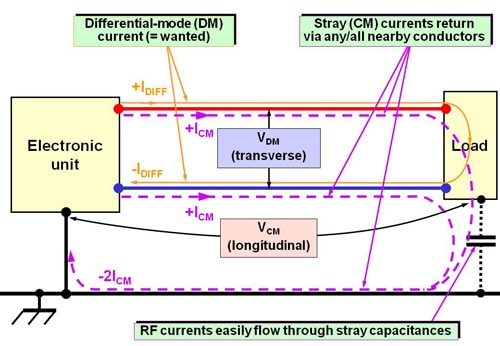
Figure 9 shows the relative paths of the DM and CM currents in a simplified system.
Paraphrasing 7.1 above – the electricity does not all stay in the wire!
Some of it travels as stray CM currents, which – like all currents – must flow in closed loops.
Because CM loops are generally very much larger than the DM loops that caused them, their E and H field patterns are much more widely spread. The result that CM is generally the major cause of “accidental antenna” effects causing EM problems for emissions and immunity over the frequency range from 1MHz to 1GHz.
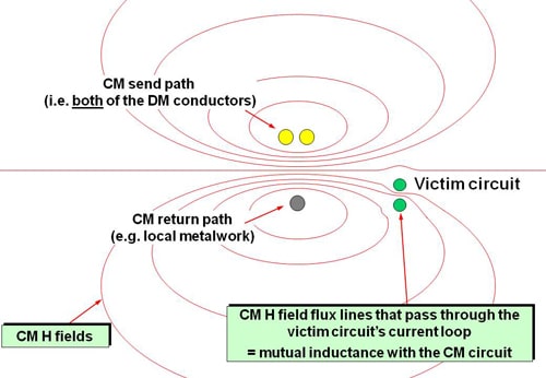
Figure 10 shows that CM currents also couple with “victim” circuits through H-field coupling, similar to how DM currents couple (in Figure 6).
Reducing the size of the CM loop reduces its H-field coupling into the victim, in the same way that reducing the size of the DM loop does in Figure 6. And reducing the size of the CM current loop also reduces the amount of E-field coupling into the victim, in the same way as for the DM E-field in Figure 5.
So, just as it is important for good SI, PI and EMC to minimize the area enclosed by all wanted (DM) current loops, it is also important for all unwanted, accidental, CM current loops. For more detail on this topic, see Chapter 5.5 of [6], 2.7.5 of [7] or 10.1.5 of [10].
Resonating Conductors Make Perfect Accidental Antennas
There are various causes of resonances in conductive structures, at certain frequencies…
a) When the L and C reactances happen to be equal
b) Due to geometry interacting with wavelength
The second item concerns transmission-line matching. When mismatched conductor characteristic impedances cause propagating waves to be reflected, under certain conditions and at certain frequencies they can cause standing waves to arise, which are a type of resonance.
At resonant frequencies, loop impedances fluctuate wildly, in the range between the conductor’s series resistance (possibly just a few mΩ), up to the stray shunt resistance (possibly a few MΩ).
Accidental antenna effects (stray couplings, whether near-field or far-field) are significantly amplified by resonances, often between 10 and 100 times (20 to 40dB), possibly more, affecting both emissions and immunity equally due to the Principle of Reciprocity.
There is No Such Thing as “Earth” or “Ground” for SI, PI and EMC
Currents always flow in closed loops. So the idea that the earth/ground electrodes provide a perfect zero-impedance sink that we can use to absorb, or otherwise make unwanted electrical power, signals or noises go away, can’t possibly be true – it is a total myth, pure and simple, having no basis in reality in this universe. [13] has more on this, especially its slides 32, 33 and 79.
Even if a zero-impedance earth/ground could exist (which it can’t, because everything has impedance) – if we sent some unwanted current into it, the current would come back via some other route to complete its loop. So, then: no current sinks (in this universe).
Earth/ground is only a valid concept (can only have any effect) for human safety, where it an issue of preventing electric shock by limiting the maximum potential differences that someone could come into contact with, whether they are caused by mains electricity leakage currents or faults, or lightning strokes.
Even when earth/ground electrodes are doing their thing for safety reasons, the relevant currents still flow in closed loops.
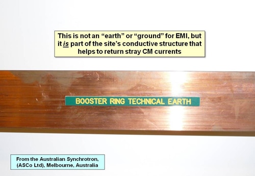
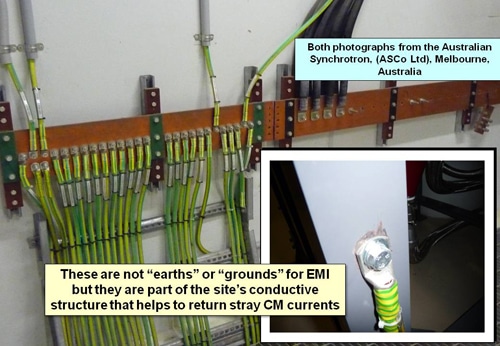
Figures 11 through 14 show some examples of what are commonly called earths or grounds, but are really just elements of a product’s, equipment’s, building’s or site’s conductive structures that help return CM currents back to their sources. Whether these structures are connected to safety earth/ground electrodes, or not, is of no consequence for SI, PI or EMC.
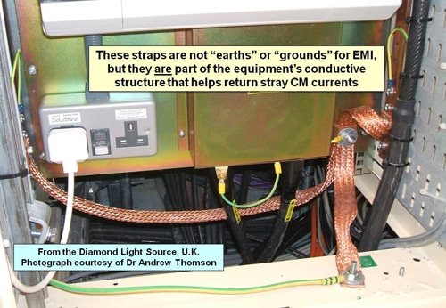
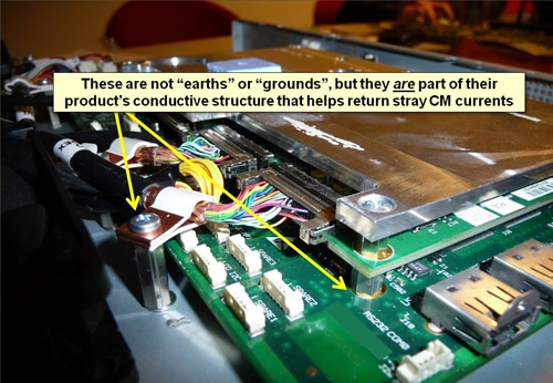
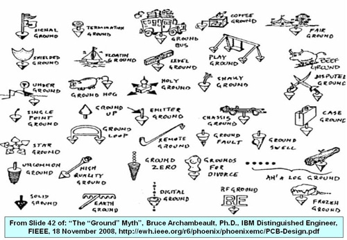
Of course, I am not the first person to comment on the meaninglessness of the term earth or ground for SI, PI and EMC. Dr Bruce Archambeault is an IBM Distinguished Engineer and a mainstay of the IEEE EMC Society, and many years ago he produced the graphic copied in Figure 15, as a way of making the same point, but in a more amusing way, see [13].
Because it is natural to assume that something called “earth” or “ground” is an infinite sink for noise currents – even though such a thing simply cannot exist – the use of such words or their graphical symbols encourages incorrect design for SI, PI and EMC, and I have seen millions of dollars have been wasted over the years for this exact reason.
So I always strongly recommend that the words “earth” or “ground” and their graphical symbols are never used in electronic design (except when a safety earth or ground is actually intended – and then for electrical safety purposes only). Instead, call the conductive structures by other names that mean what they say, e.g. RF Reference (see 8 below), CM Return Path, or whatever.
Using words such as “chassis”, “frame”, “enclosure”, “shield” or “Faraday Cage” can also lead to the same conceptual design errors as “earth” or “ground” – so it is important to be very careful to only use them to mean what they actually are (i.e. mechanical structures made of metal) rather than assume they are (mythical) infinite sinks for noise currents.
For more detail on this, see 5.7 of [6] or 2.7.7 of [7], also 11.1.2 and 11.1.3 of [10].
APPLYING THESE “EM DESIGN TOOLS” TO A REAL-LIFE PCB ASSEMBLY
Introduction to the Example
Sections 2 to 7 above have given us a set of EM design tools – really just mental concepts for how the EM energy that we call our power and signals actually prefers to flow to maximize SI, PI and EMC.
Notice that in sections 2 through 7 I intentionally used very little math; it is not necessary for an understanding of these important concepts. In fact, using equations can obscure what is really going on, which every successful EMC designer learns to “see” with his/her “mind’s eye” just by looking at the conductive structure of a product.
With the complexity of modern products it is best for the designer to understand the concepts and have “the eye” for them, leaving the calculations to the appropriate types of EM field solvers.
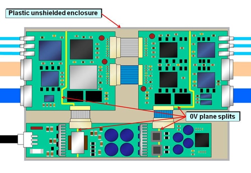
Anyway, now for a real-life example – controlling the EM emissions and immunity of the typical electronic product sketched in Figure 16.
To minimize the overall cost of manufacture, this PCB assembly should have good EMC characteristics, so that a lot of money and time does not have to be spent (and add weight and size) by shielding and filtering it to get it to pass its EMC tests.
Because our EM design tools are all concerned with controlling EM field patterns to minimize unwanted “noise” coupling, the exact same tools also improve immunity (e.g. maximizing immunity to nearby walkie-talkies, cellphones, GPRS, 3G, Wi-Fi and Bluetooth transmitters, and also transients, ESD and lightning).
The assumptions made in the initial design of the example were not in accordance with the “Laws of Physics Based EM Design Tools” outlined in 2 through 7 above. Instead, they represent what are unfortunately still commonplace bad practices in many electronic product design departments.
One bad practice used in our example is the use of so-called “single-point earthing/grounding” (sometimes called “star earthing/grounding”), using 0V plane splits between (and on) the PCBs. This is assumed to keep devices’ circulating return currents confined to certain circuit areas, preventing crosstalk of noise between them (e.g. digital noise in analogue) – but it only works well below a few tens of kHz.
Splitting 0V planes ignores the fact that fluctuating currents always divide up according to the admittances of the various alternative paths, including “stray” paths through the air or insulation (see 7.1 above). For this reason, since 1980, the author has always found that when microprocessors and switch-mode converters are used, single-point earthing/grounding has always been a bad design practice for SI, PI and EMC. Others will no doubt be able to give examples from before 1980.
Another bad design practice used in the example is the assumption that achieving the lowest BOM cost is sufficient to produce the most profitable product. So the number of board layers and amount of power decoupling was reduced to the minimum that achieved the functional specifications. Also, provision has not been made for fitting EMI filters to all of the cable connections, because this would have increased the board’s area.
Section 1 mentioned that relying on achieving the lowest BOM cost to create profitable products has been known to be an incorrect practice since 2000. Plain common sense easily reveals the fallacy inherent in this overly-simplistic approach – we only have to consider a product that had a BOM cost that was half (or less) of that of all its competitors – but suffered a 100% warranty return rate. Clearly, this would not be a successful product, so there is very much more to a product’s profitability than its BOM cost.
I see many designs like the example in Figure 16 every year. They all suffer poor functional performance at first, especially poor signal-to-noise (S/N) ratios and unreliable software that take many design iterations to solve, causing project delays, increasing costs and reducing profitability.
Once the functional problems are solved, they then fail their EMC tests, requiring many more design iterations to solve, causing more delays and more project costs, plus requiring the addition of filters and shielding that increase BOM cost, weight and size and reduce profitability even more. They also suffer higher-than-hoped-for warranty return rates, which erode profitability even more.
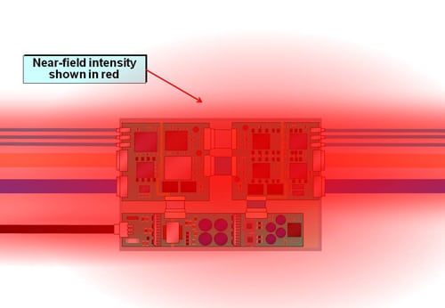
A plot of the near-field emissions 20mm above the PCB assembly, at the stage where it meets its functional specifications but has not yet been tested for EMC, is shown in Figure 17.
What do such near-fields mean? This close to the PCB and its components they are the wanted DM signals, plus DM and CM crosstalk and noise. High levels mean reduced S/N ratios in analogue circuits, and reduced noise margins in digital circuits – leading to unreliable software.
In EMC testing, high levels of near-fields over large areas indicate high levels of conducted and radiated emissions, and correspondingly poor conducted and radiated immunity.
In real life, high levels of near-fields over large areas means a lower proportion of satisfied customers (increasing the cost of future sales, because it is easier to sell products that customers like), and higher levels of warranty costs. All causing lower profitability.
We understand, from the laws of physics discussed in sections 2 through 7, that:
• all currents (including DM and CM “noise” currents) flow in closed loops
• current loop shape and area govern field patterns
• currents naturally “prefer” to flow in the loops that have the lowest impedance – hence the smallest field patterns and best internal and external EMC.
So we can see how to make a number of improvements to the circuit design and PCB layout, to reduce the areas of the DM and CM current loops and make their near fields more compact.
Improvement #1: Create an RF Reference
We replace the multiple PCBs, with a single PCB that has a common conductor (almost always a 0V plane) over its entire area, which I shall call the RF Reference. You may choose your own name for it, as long as it is not “earth” or “ground”.
The RF Reference in a PCB is at least one solid, continuous, copper plane layer, which lies underneath – and extends well beyond – all devices, components, traces and power plane areas.
There should be no traces “snuck into” this plane layer, and any gaps in it must be unavoidable and as small as possible.
Cellphone designers found that their products’ close proximity between 2 Watt UHF or microwave RF transmitters, microphone amplifiers and digital processors meant that even the clearances around via holes added too much impedance to their RF Reference planes, so developed microvia PCB manufacturing technology (also called “High Density Interconnect” or HDI, or “Build Up”) that provides 100% solid copper RF Reference planes.
An RF Reference achieves very low impedance (Z), the value of which depends on the devices and the EMC requirements specification to be met – but it must always be <<1Ω over the frequency range that must be controlled to avoid causing/suffering EMI.
“The frequency range that must be controlled to avoid causing/suffering EMI” is all of the DM frequencies created in the devices on the PCB, and all of the frequencies existing in the operational environment and/or in the immunity test standards (if they require immunity over a larger frequency range).
Designing a profitable product is all about satisfying customers whilst selling a legal product at an overall profit, and there can be many more EMI requirements involved in satisfying customers than merely passing the minimum requirements of the minimum set of EMC test standards required for legal sales.
The point of creating an RF Reference is that it automatically provides a low-impedance (high-admittance) return path for all possible power/signal/noise currents, and CM noise currents on the PCB. Because it is in very close proximity to the PCB’s components, devices and traces, all these current loop areas are small – just what we need for good SI, PI and EMC.
It is important to realize that we don’t have to “make” the return currents flow in the RF Reference and so have the least E and H field emissions – we only have to provide an RF Reference plane and they will naturally “prefer” to flow in it rather than elsewhere! (See Figures 7 and 8). The RF Reference plane works best with lower-profile components, so we also replace any tall components and devices with ones that lie close to the PCB and its RF Reference plane layer(s).
See Chapter 7.4 of [7], 3 and 4 of [12] and 11.2.2 of [10] for more detail on creating effective low-impedance RF Reference Planes in PCBs.
Improvement #2: Decoupling the DC Supplies
We design the decoupling between DC power rails and the RF Reference to achieve low Z, the value of which (as for 8.1) depends on the devices and the EMC requirements specification to be met – but must always be <<1Ω over the frequency range that must be controlled to avoid causing/suffering EMI.
This permits the fluctuating DM currents in the power rails to flow in much smaller loops very close to the devices that cause them – which they naturally “prefer” to do, rather than flowing more widely in the RF Reference – making small areas of DM near-fields that create less CM noise emissions than larger areas would.
PC motherboards now need to achieve power supply impedances of much less than 0.25 mΩ to frequencies much more than 1GHz. This is impossible to achieve with low-cost decoupling capacitors, because above about 300MHz they are beyond their self-resonant frequency and so act inductively – their impedance rises with frequency – making low-enough impedances impossible.
However, because we now have a RF Reference plane in the PCB, we can pair it with adjacent power planes to provide distributed decoupling capacitances within the PCB’s fiberglass dielectric, which can maintain very low impedances up to any number of GHz.
See Chapter 7.5 of [7], 5 of [12] and 12.1.3 of [10] for details on how to do effective decoupling on PCBs.
Improvement #3: Cable Filtering
We add direct bonds or filters to the RF Reference on all traces connected to off-PCB conductors, whatever their electrical/electronic/other purpose (including metal mechanical parts; and metal hydraulic/ pneumatic pipes, etc.).
Filters on inputs can often be just a capacitor connected to the RF Reference, but filters on outputs will generally need a series resistor or soft-ferrite choke so that adding the capacitor to the RF Reference does not significantly increase the peak output current.
Of course, we might need to make more complex filters by combining capacitors with resistors and/or soft-ferrite chokes and/or CM chokes – but there are far too many details involved to even start to address this topic in this article. For more details on filtering, see Chapter 5 of [7], 2 of [12] or 13.2 of [10].
These direct bonds or filters are placed where the traces connect to the off-board conductors, to provide low-Z paths for CM currents that would otherwise “leak” from the PCB into the conductors. As for 8.1, the values of Z that are required depends on the devices and the EMC requirement specification, but must always be <<1Ω over the frequency range that must be controlled to avoid causing/suffering EMI.
Improvement #4: Using Matched Transmission Lines
Where device data sheets specify the use of matched transmission-lines – usually for high-speed clocks or serial data lines – designers almost always remember to control their trace geometry and matching impedances.
But they generally do not consider treating all of the other traces as matched transmission lines, until they are investigating digital signal over/undershoots, ringing or other unwanted noises that cause incorrect or unstable software operation late in a project – the stage where delays and design changes are most costly.
These over/undershoots or ringing are indications of strong emissions (and poor immunity at the emission frequencies), as shown in [2]. Suppressing them to get good EMC, either by filtering at their drivers or by using matched transmission lines to reduce “accidental antenna” effects and prevent resonances, results in very low over/undershoots and no ringing. It also reduces crosstalk and makes (bug-free!) software work very reliably indeed.
EMC textbooks often make recommendations about when to treat a PCB trace or cable as a matched transmission line, but digital device rise- and fall-times are now generally so short (typically < 0.5ns for 74-series glue logic and < 0.2ns for microprocessors and memories) that almost all practical trace and cable lengths now need either to be filtered to significantly reduce their frequency content, or else be treated as matched-impedance transmission lines.
See Chapters 4.7 and 7.6 of [7] and 6 of [12] for more on designing with matched transmission lines.
The Improved Example
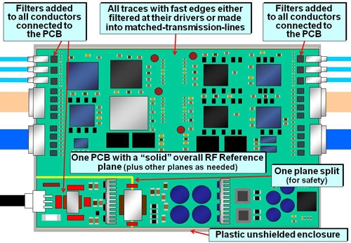
The appearance of the example PCB improved by 8.2 through 8.5 above, is shown in Figure 18. Notice that it still has one plane split, under the mains safety isolation transformer – which cannot be avoided.
Despite increasing the number of board layers to provide RF Reference and Power Supply planes, and additional planes for controlling transmission-line impedances, and despite increasing the number of decoupling capacitors and filters, it is quite normal to find that the overall cost of manufacture (not the BOM) is lower. This is because the inter-board connectors and their cables have been removed – significant causes of assembly errors and rework; unreliability and warranty returns.
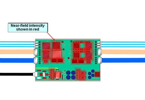
Figure 19 shows the near-field plot 20mm above the improved PCB assembly, which now has only small red areas around the components. These are almost entirely the DM fields associated with the wanted power and signals, which we cannot eliminate without eliminating the power or signals themselves.
Remember, all fluctuating currents (whether power, signals or noise) are really EM energy propagating as waves, so the best we can do is provide structures that allow these currents to naturally flow in loops of low impedance (high admittance) so that they naturally create very small and local field patterns, with great benefits for SI, PI and EMC. When we have achieved this, as shown in Figure 19, we see very little field-spreading is seen due to CM noise currents.
Improving by Using Cable Shielding
Where the use of filtering and unshielded cable techniques (Chapter 4.4 of [7], 2 of [12] and 13.1.8 of [10]) could not suppress the DM or CM fields around a cable by enough, shielding might be necessary for some (or all) cables and/or parts of (or the whole) PCB assembly.
CONCLUSIONS
All electrical and electronic activities are really EM energies travelling as propagating waves, and connecting to safety earth/ground has no effect on them so is unimportant and unnecessary for SI, PI and EMC.
We can easily design circuits and PCBs to create small, low-Z current loops for both the wanted DM and the stray CM currents, the EM waves naturally prefer to flow in these routes. So, by working with the laws of physics, we automatically achieve very compact field patterns, which are best for internal and external EMC and financial success.
Because these techniques control field patterns to minimize unwanted “noise” coupling, because of the principle or reciprocity the exact same techniques also minimize susceptibility, for example minimizing unwanted “noise” couplings.
The principles of good design techniques for SI, PI and EMC are very clear, easy to understand, and easy for everyone to implement at low cost in practice. Products really are doing their best to help us pass EMC tests and meet EMC requirement specifications – all we need to do is give them a little help, from the start of their design process.
10. REFERENCES
[1]. Armstrong, K. “Key knowledge for the efficient design of electronic products and their EMC – that we were never taught at university”, Keith Armstrong, ANSYS Seminar “Next Generation Signal Integrity and EMI Simulation”, 23rd March 2011, Oxford, UK. www.ansys.com/staticassets/ANSYS%20UK/staticassets/Keith_Armstrong_Presentation_ANSYS_March_23%202011.pdf
[2]. Armstrong, K. “EMC and Signal Integrity,” Compliance Engineering, March/April 1999.
[3] “The Consumer Electronics Boom — How Semiconductor and Consumer Electronics Companies Can Improve Cost, Time-to-Market, and Product Quality,” KPMG LLP’s Information, Communication and Entertainment (ICE) Practice, 2008.
[4] Armstrong, K. “BOM cost, and profitability,” The EMC Journal, May 2009, pp 32-34.
[5] Armstrong, K. “Maxwell’s Equations, Quantum Electrodynamics, and good installation practices for SI, PI and EMC,” The EMC Journal, Issue 91, November 2010.
[6] Armstrong, K. “The Physical Basis of EMC,” Armstrong/Nutwood UK, October 2010, ISBN: 978-0-9555118-3-7.
[7] Armstrong, K. “EMC Design Techniques for Electronic Engineers,” Nutwood UK November 2010, ISBN: 978-0-9555118-4-4.
[8] http://en.wikipedia.org/wiki/Vacuum_state
[9] Feynman, R.P. “QED The Strange Theory of Light and Matter,” Penguin Books, 1990, ISBN: 0-14-012505-1.
[10] Williams, T. “EMC for Product Designers, 4th Edition,” Elsevier 2007, ISBN-10: 0-750-68170-5, ISBN-13: 978-0-75-068170-4.
[11] Klinger, M. “Modeling and Simulation of Powertrains for Electric and Hybrid Vehicles,” Workshop FR-AM-4-1, IEEE 2009 International Symposium on EMC, Austin, TX, Aug 17-21, 2009.
[12] Armstrong, K. “EMC for Printed Circuit Boards – Basic and Advanced Design and Layout Techniques,” Nutwood UK December 2010, ISBN 978-0-9555118-5-1.
[13] Archambeault, B. “The ‘Ground’ Myth”, 18 November 2008, http://ewh.ieee.org/r6/phoenix/phoenixemc/PCB-Design.pdf
Keith Armstrong graduated from Imperial College, London, in 1972 with an Honours degree in electrical engineering. He has been a member of the IEE since 1977, a UK Chartered Engineer since 1978, and a Group 1 European Engineer since 1988. He founded Cherry Clough Consultants in 1990. Keith can be reached at keith.armstrong@cherryclough.com.
