This article is part 2 of a three-part Filter Installation Issues series. Read Part 1: Input and Output Conductors here.
Some mains filter manufacturers only design and specify their filters to provide attenuation over the frequency range of the conducted emissions tests (typically up to 30MHz for commercial and industrial products), to keep costs low. Unfortunately, if such filters have poor attenuation above 30MHz, they will degrade the shielding effectiveness (SE) of a shielded enclosure above that frequency by permitting RF signals to leak out via the filtered cables – resulting in problems for both emissions and immunity.
It does not matter what is the ostensible purpose of a conductor, e.g. mains or DC power, audio, whatever – if its filtering and/or shielding provides less attenuation than is required for the shielded enclosure, it will degrade the SE of the enclosure. The filtering and/or shielding of cables used for audio, mice or keyboards are often ignored when they exit a shielded enclosure. The assumption is usually that the signals they carry will not cause a problem for EMC.
But this overlooks the fact that all conductors or whatever type or signal designation always behave as ‘accidental antennas’ (see [1]), very readily picking up EM noises on either side of a shielded barrier and retransmitting them on the other side – unless specifically prevented from doing so by the application of shielding and/or filtering.
If good high frequency shielding is required, all unshielded cables that enter the enclosure (including mains) must be filtered with good attenuation at the highest frequency of concern for shielding purposes. So where shielding is required up to 1GHz (for example), only employ filters with data showing good attenuation up to at least 1GHz.
Few mains filters intended for commercial and industrial equipment specify attenuation above 100MHz, so additional high-frequency filtering might be needed. However, some filter manufacturers (e.g. EMC Solutions) specify their filters up to 1GHz.
Assembly and Installation Techniques for Filters that Penetrate Shields
As discussed above, the performance of shielded enclosures can easily be degraded by RF noise that ‘leaks’ out along the cables that enter and exit the enclosure. The shielding/filtering synergy issues discussed above are vital considerations when high levels of shielding or filtering are required (e.g. >40dB) at frequencies >100MHz.
The design of shielded cables was covered in [1], and the design of shielded enclosures will be covered in a future installment of this series. This section discusses how filters should be installed in shielded enclosures so that they do not permit RF noises to pass through them that could compromise the SE of the enclosure.

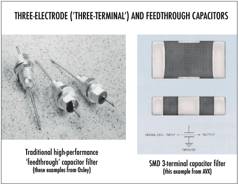
Figure 1 shows an example of a ‘feedthrough’ capacitor specifically designed for use where unshielded conductors penetrate a shielding enclosure, which could be a product’s enclosure or an internal shielded volume.
Feedthrough capacitors have three terminals, for input, output and ‘ground’. The signal to be filtered enters at one side of its electrodes and exits at the other, having to pass the ground electrode as it does so.
The middle ‘ground’ terminal connects directly to the shield, using a 360° electrical bond so that the internal and external surface currents stay separated on either side of the shield, as shown in see Figure 19, allowing the shield to function correctly.
If designed correctly, the shielded enclosure prevents stray coupling between the capacitor’s input and output terminals, and also provides the filter with an RF Reference Plane with negligible impedance at the highest frequency of concern, all of which helps the filter employing the feedthrough capacitor to achieve the best performance it is capable of.
When used as (or in) filters, traditional feedthrough capacitors such as the ones shown in Figures 21 and 1 provide much better attenuation, at much higher frequencies, than is possible by using ordinary two-terminal capacitors. Traditional feedthrough capacitors are soldered or screwed into a shield wall and connected to the circuits on either side by wire conductors. They are often used between shielded compartments within RF equipment, e.g. to filter the DC power that passes between the RF, IF and digital sections of an RF receiver or spectrum analyser.
Traditional feedthrough filters, such as those shown in Figure 3W, are also available as ‘filter pins’ in some standard connectors, such as some D-types and military circular connectors. (Note that not all connectors with builtin filters use feedthrough filter pins, some use discrete components on miniature internal PCBs, which will not achieve as good an attenuation at the highest frequencies.)
Traditional feedthrough filters are not favoured for modern volume-manufactured products because of their high component cost, and the high cost of their manual assembly and the assembly of the wires they connect to.
Volume-manufactured products prefer to use SMD components automatically assembled on PCBs – but since a true feedthrough capacitor cannot be automatically assembled, three-terminal capacitors have been developed to fulfil this purpose.
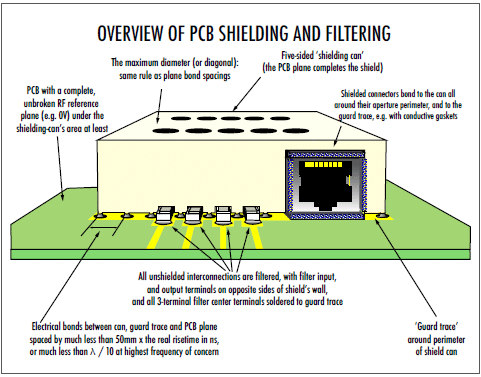
Figure 1 includes an example of a three-terminal capacitor intended for SMD assembly processes, and Figure 2 shows an example of how it is used in conjunction with PCB shielding. The capacitor is aligned with the shield wall so that its input and output terminals are shielded from each other by the PCB-mounted shielding-can, and the capacitor’s centre ‘ground’ terminal is soldered directly to a guard trace that follows the wall of the shield-can and connects it to a PCB plane (almost always 0V) with a wall of via holes.

The gaps that are cut out of the shield-can’s wall for the bodies of the filters are known as ‘mouseholes’ (for reasons that should be obvious to anyone who enjoys ‘Tom and Jerry’ cartoons). Three-terminal capacitors and the filters that use them cannot be as good as proper 360° shield-bonded feedthrough types, because there will always be some stray coupling through the mouseholes in the shield.
But careful control of the maximum dimensions of the mouseholes, and of the spacing between the via-holes connecting the shield wall to the PCB plane that provides the shield’s sixth side, can nevertheless achieve excellent performance. For more details on this, see Part 2 of [2].
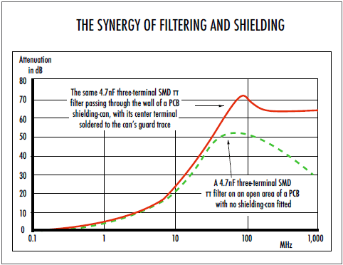
Figure 3 shows attenuation of a three-terminal SMD π filter assembled on a PCB, and the effect of adding a PCB-mounted shielding-can in the manner shown in Figure 2.
Without the PCB’s shield-can fitted, the filter performance is quite respectable at about 50dB at 100MHz, but above that frequency it falls off at 20dB per decade, so that it is only about 30dB at 1GHz, and it would presumably be about 10dB at 10GHz.

But the addition of the shielding-can reduces the stray coupling bypassing the filter very considerably, and also allows correct separation of internal and external surface currents and provides an RF Reference Plane that has a much lower impedance over the frequencies measured.
The result is an attenuation of around 70dB at 100MHz, and a more-or-less flat attenuation that maintains about 65dB up to 1GHz – easily 35dB more attenuation than was achieved without the shield. It is not clear what the performance with the shield-can would be above 1GHz, but as there is no sign of any roll-off even at 1GHz it is likely that an attenuation of at least 45dB would be achieved at 10GHz.
As described in section 2.6 of [1], shielded cables exiting a shielded PCB region require shielded connectors or glands that are electrically bonded to the shield-can’s wall by mechanical fixings, soldering or gasketting that makes multiple connections around its periphery – preferably full 360° bonding.
The experiment whose results are shown in Figure 3 reveals two important things:
- Filters that must provide significant levels of attenuation at frequencies above 100MHz, must employ shielding techniques as well. They will not be able to achieve the required performance otherwise.
- Modern digital ICs produce large amounts of CM and DM noise at frequencies above 1GHz, and products supplied to the USA already have to comply with FCC emissions limits above this frequency. The EN standards used to achieve a presumption of conformity with the EMC Directive for products supplied to Europe will soon be changing to include emissions and immunity requirements above 1GHz – at least to 2.7GHz and maybe higher. To comply with these requirements using low-cost SMD PCB assemblies will require the use of shielding wherever GHz frequencies need to be filtered.
REFERENCES
[1] Keith Armstrong, “Design Techniques for EMC, Part 2 – Cables and Connectors”, The EMC Journal, May and July 2006, available from www.compliance-club.com.
[2] Keith Armstrong, “EMC for Printed Circuit Boards – Basic and Advanced Design and Layout Techniques”, February 2007, www.emcacademy.org/books.asp, £47 plus p&p, perfect bound: ISBN 978-0-9555118-1-3, spiral bound (lays flat): ISBN 978-0-9555118-0-6