Introduction
The increasing use of electronics in vehicles introduces new risks of interference and crosstalk between components. OEMs and government regulators impose strict limits on electromagnetic interference (EMI) and electromagnetic compatibility (EMC), and redesigning a component that fails to meet these standards can be both expensive and time-consuming. This article explains how electromagnetic simulation can be used to design and analyze automotive Ethernet systems to identify and mitigate EMI/EMC problems early in the design process, reducing the risk of problems emerging later.
Background
The number of electronic components in the average car is growing and smart vehicles are a major driver of growth in the automotive market. Designing an electronic system always poses a challenge to the electronic engineer, but there is an additional challenge in the need to connect all of them. To achieve this connection of data between these electronic systems, communication standards are needed.
Modern electronic systems like advanced driver-assistance systems (ADAS) and infotainment have a very high bandwidth requirement, for example for video streaming. The traditional vehicle bus protocols like Controller Area Network (CAN) are not able to provide this bandwidth and there is a need for a new standard with high bandwidth. Automotive Ethernet is a very promising candidate to fill this gap.
Ethernet has been well known for several decades as a connectivity solution in buildings but had not been used in vehicles due to the prohibitive bulk and weight of the cables. Traditional Ethernet cables typically consist of 4 twisted wire pairs (TWPs) that may also be shielded. To develop automotive Ethernet, the physical interface was simplified to one unshielded TWP while keeping the other components of the Ethernet bus the same. These unshielded twisted cables have data rates of 100 Mb/s and are lightweight and cost-effective.
Broadcom created the BroadR-Reach standard for automotive Ethernet [1] and to promote its use, the OPEN Alliance (One Pair Ether-Net) was created [2]. Most major players in the automotive market now participate in this alliance. BroadR-Reach® is a point-to-point Ethernet Physical Layer standard for automotive applications, allowing full-duplex communication between two devices over an unshielded twisted wire pair at 100 Mb/s, with plans to further increase it to 1000 Mb/s. However, they make compliance with the BroadR-Reach® Ethernet with automotive EMC requirements a challenging task.
EMC compliance is crucial for releasing products to the market. Regulators such as the FCC and ETSI set EMC limits, and if a product does not comply with them, it cannot be sold in the given country. Furthermore, manufacturers can impose even stricter standards on their suppliers, which can vary from OEM to OEM.
Traditionally, EMC testing has been heavily reliant on measurements with physical prototypes, which can lead to multiple troubleshooting iterations with high corrective costs and delayed time to market. Identifying potential EMC issues earlier on in the design process can offer significant savings of time and investment. Simulation can be used at any stage of design to model and visualize currents and fields in order to help engineers find and mitigate EMC issues. This can reduce the number of physical prototypes needed, along with reducing the risk of delays, increased costs or embarrassing recalls due to unforeseen interference issues.
PCB Setup
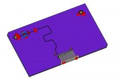
This example (Figure 1) uses a typical driver IC for automotive Ethernet (NXP TJA1100) [3]. A PCB stack up was designed using Altium Designer and the Ethernet routed as a differential pair to a simplified connector. The termination on the Ethernet channel is a second PCB, identical to the first one.
A coupled 3D field and circuit simulation were used for this example. This co-simulation is a very common workflow for EMC simulation. The PCB and cable model was analyzed over a frequency range from 0 to 200 MHz, using the Frequency Domain solver in CST Studio Suite® [4], which is based on the finite element method (FEM). An AC frequency domain simulation was used for the circuit.
At frequencies above 1 MHz, the BroadR-Reach automotive Ethernet carries a much higher spectral content than the CAN bus. Designers need to be aware of this and apply the proper techniques to mitigate emissions at these higher frequencies.
Common and Differential Mode
As the automotive Ethernet is run on a differential pair, there are two possible propagation modes: the common mode and the differential mode. While the differential mode is the one used for signaling, the (unintended) common mode will always be created in the system due to asymmetries and is often the source of unwanted electromagnetic emissions. Simulations using multipin waveguide ports can be used to look in detail at the modes and to visualize the electric and magnetic field patterns.
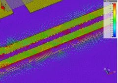
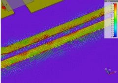
Figure 2 shows the surface current at 33 MHz. In the differential case, the current flows in opposite directions on both lines, while for the common mode the current goes in the same direction and therefore has to flow back to its source in the (common) reference plane. A close look at the bottom image of Figure 2 shows that there will still be some current on the reference layer in the differential case, albeit with a much smaller amplitude than in the top image.
In the connector, the differential mode is mostly confined to the TWP, while the common mode arises between the TWP and the power (PWR) and ground (GND) wires. If the loop area of the common mode is large, this may lead to higher coupling, higher emissions, and to insufficient electromagnetic compatibility (EMC).
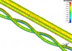
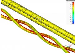
As shown in Figure 3, the differential mode flows on the inner section of the TWP, while the common mode flows on the outer side, close to the PWR and GND wires. This plot emphasizes the high accuracy of the full-wave 3D solution. Electromagnetic effects can be visualized, and even the position of the mode on the cable is taken into account.
To summarize, the differential to common mode conversion occurs due to non-ideal symmetry in the transmission lines. One cause of these asymmetries can be jitter and skew in the signal generation, which depends on the silicon driver used. Designers may have limited access to models for the driver but can account for this in other ways in the simulation model. Another possible cause is asymmetries in the geometry. These can appear due to routing, connector and cable bonding, and other physical discontinuities. We will look at these factors in the next section.
Conducted Emissions
In a typical automotive test set up, the device is connected by cables to a line impedance stabilization network (LISN). The conducted emission is measured at the LISN port. In the first model with just the PCB and the connector, the conducted emission levels are quite low.
However, the real system will have cables connected to them. To account for this, a 1 m long cable is attached to the simulation model. The Ethernet lines are twisted, the PWR/GND are straight. After adding the cables, the emission level increases at the 40 MHz mark by about 20 dB.
Changing the distance between the PWR/GND and the TWP wires causes only little changes in the emission. Even putting the power wires at a 90° angle to the TWP only reduces the emission by a few dB, as shown in Figure 4 (brown line). The reason is that the emission in this example is dominated by the common mode which is created mainly on the PCB and the connector. As the cables in the simulation are connected to an ideal metallic box with no losses, the common mode can flow very efficiently from the TWP to the PWR/GND pair. The separation of the cables has only a small effect.
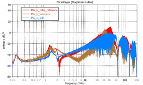
A much bigger effect is caused by using different references for the TWP and the GND. When the PWR/GND is connected to a different reference from the TWP, the emission drops significantly as shown in Figure 4 (blue line). The measurement standard prescribes that a common reference needs to be used so this is not a way to mitigate the emission. However, it is important to understand this link because it is a direct effect of this measurement set up.
A way for designers to reduce the emission in practice is by changing the connector pinout. The PWR/GND pair in the simulation was split and put on opposite ends of the connector, creating a wide connection. The emission is significantly increased under this set-up, especially at lower frequencies, due to the fact that the loop created by the PWR/GND is now much bigger.
The effect of untwisting can also be investigated. The TWP is typically untwisted close to the connector in order to bond the wires to the connector pins. Two untwisting scenarios are tested: a short untwist giving a 2.5 cm straight section and a long one giving a 5 cm straight section. We can observe the strong effect of increasing the length of the untwisted wires (Figure 5), leading to problematic increases in emission.
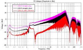
Finally, a worst-case scenario is considered, in which there is a wide connection across the connector, a long section of untwisted TWP and where the routing on the PCB is not fully symmetric. With all these changes, the emissions increase by approximately 30 dB across the whole frequency range. It is important for the designer to understand what values can be reached with which design changes, and where additional components are needed.
Countermeasures
One of the main countermeasures against emission is a common mode choke (CMC). This section will investigate in which cases the CMC is helpful. A CMC is a special coil that has a low impedance for the differential mode and a high impedance for the common mode. Thus, it should block the common mode and let the differential mode pass.
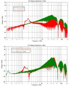
Figure 6 shows the effect of a common mode choke (CMC) on the EMC performance of the system. At the receiver (upper plot), the choke reduces the common mode as expected. However, at the LISN pin (lower plot), the choke did not have a big effect. There is a difference between the choke effects because there is a difference with how the common mode is created in these two locations.
It has been discussed how common mode emission is caused by asymmetries in time or geometry in the model. In order to simulate the asymmetries in time that cause common mode noise, we need to change from the AC simulation to a transient circuit simulation. We add an asymmetry in the time signal, so there is a skew in the driver: the negative voltage is 0.1 ns later than the positive voltage.
Driving the model including the CMC with the skewed signal reveals that the emission is almost the same for the skewed model as for the model without skew. Removing the choke while the signal has a skew causes emission to drastically increase. Thus, the CMC does an excellent job of suppressing the common mode due to the skew.
However, if we consider the geometry of the setup, one CMC is placed on the reference PCB and the other on the termination PCB, with a long signal path between them. If the common mode is created along this path, it will not be filtered and it can couple to the PWR/GND wire pair. This is why the CMC does not help much to reduce the common mode created by the untwisting.
Another possible way to reduce emissions is to use a ferrite clamp. This can be simulated as a ring of high permeability material or with more realistic material models by using the “Ferrite macro” in CST Studio Suite. The ferrite ring may reduce the emission or may move the emission peak to lower frequencies.
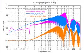
An alternative countermeasure is adding shielding. In this case, the bonding of the shield is very important. When an ideal shield is connected to the ground layer of the PCB in a 360° fashion, the shield works excellently and suppresses the emission by about 40 dB.
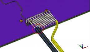
However, this kind of ideal shielding is not possible in the real connector. Instead, the shield is bonded to a connector pin as shown in the red circle in Figure 7. In this more realistic bonding scenario, the effectiveness of the shield drops dramatically: the improvement is now only about 10 dB.
Often in the automotive industry ferrites and shields are not an option because they offer only modest improvements and add too much weight and cost. As the common mode choke is already present in the system, it is important to understand how it functions and what its effect on the emission is.
Radiated Emissions
Field probes are used to measure the radiated emission in simulation. A sphere of probes is generated with a radius of 1 m from the device under test. Then the emission at all probes is calculated and the worst-case envelope is extracted in a post-processing step. This is similar to the way a physical measurement is made but, in order to increase speed and efficiency, it does not take into account the real antenna used for the measurement. All these steps can be automated as macros within CST Studio Suite.
Changing the connector layout does seem to be much less critical for radiated emissions than it was in the conducted emission case. On the other hand, untwisting the cables causes similar behavior to the conducted emissions case: The longer the section of untwist is, the higher the emission.
An interesting side note is that by putting the PWR/GND cables at a 90° angle the radiated emission is actually higher, whereas the conducted emission was slightly lower. This is because this set-up produces a much larger loop of the common mode current.
Bulk Current Injection
The bulk current injection (BCI) test is an automotive industry standard for analyzing the susceptibility of electronics and simulation can also be used to access this testing standard.
A BCI clamp model is placed around the cables in the automotive Ethernet simulation. The injection is performed by a 300 mA current, which is a typical testing level in BCI. Disturbance to the actual Ethernet communication will appear in the differential mode that arrives at the receiver. It is the inverse of the emission case: in the emission case, a differential mode is injected and the common mode is typically observed. In the BCI, a common mode is injected and the differential mode is examined.
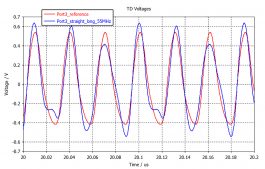
It is difficult to judge the impact on the communication by looking at the AC spectrum at the transmitter. A time domain simulation is needed to better understand the effects. The Ethernet channel is excited with a 33 MHz rectangular signal and the transmitted signal at the receiver is recorded. The rectangular pulse has been smoothed at the receiver. This is mainly an effect of the DC caps. However, the high and low levels can still be clearly distinguished in the received pulse. Even after injecting an 88MHz signal at the BCI clamp, which is the frequency at which the coupling is greatest, the signal at the receiver is almost unaffected. This indicates the BCI test will probably be successful.
If the pinout is changed to a wide connection, the coupling to the differential mode is almost the same as in the reference solution, so a changed connector layout will not have a big effect on the BCI test. However, if the wires are now untwisted, the coupling level to the differential mode increases significantly. So, as in both previous examples, the untwisting of the wires has a big effect.
Conclusion
The examples presented are all based on the coupling of the full-wave 3D model to a circuit simulation. The effect of the connector & PCB layout on the common mode and also the high impact of the untwist of the TWP at the connector have been demonstrated. The simulation of a BCI susceptibility test was also shown.
The PCB, connector, and cable all have a distinct influence on the emission, and understanding the creation of the common mode is one of the key steps in successfully designing the system. Several countermeasures to suppress the emission have been discussed. However, all emission and susceptibility scenarios have shown that the untwisting of the TWP at the connector has a very adverse effect. The untwisting length needs to be kept as short as possible.
The automotive Ethernet is a next-generation signal bus for bandwidth-intensive applications in vehicles. Because of the speed of the bus, the signals have a much higher frequency than, for example, CAN and designers need to be aware of this. Simulation can be run at an early stage of the design and give valuable answers about the EMC performance of a design.
References
[1] BroadR-Reach® Physical Layer Transceiver Specification For Automotive Applications, Broadcom, http://www.ieee802.org/3/1TPCESG/public/BroadR_Reach_Automotive_Spec_V3.0.pdf
[2] OPEN Alliance, http://www.opensig.org/
[3] TJA1100 data sheet, NXP Semiconductors, https://www.nxp.com/docs/en/data-sheet/TJA1100.pdf
[4] CST Studio Suite, www.cst.com
About the Author
Matthias Tröscher is the Business Development Executive for Transportation & Mobility, focusing on EM simulation in the automotive industry. Tröscher has worked at CST since 2009 and is currently the Business Development Manager for Germany, Austria, and Switzerland. Tröscher received his doctorate from the Johannes Kepler University Linz in 2000 for his work on radar warning systems carried out for BMW in Munich. His professional career began with the development of simulation software for analyzing PCBs and cable harnesses.
Tröscher is a member of the IEEE EMC Society and is Vice Chair of the IEEE German EMC Chapter and the IEEE Technical Committees TC-9 for Computational Electronics.
Matthias Tröscher has been involved in the organization of many automotive conferences in Korea, Germany, and the U.S.A., and has produced articles for magazines, journals, and conferences.


