Note: The below article has been translated from German and can be found in its original language in the 2012 EMC Europe Guide.
Part 1 of this article can be found here.
INTRODUCTION
The successful development of electronics with good EMC characteristics today largely depends on the EMC behavior of the ICs used.
Part 1 of this paper, titled “Pulse Immunity of ICs in Different Packages,” showed that the some ICs behave differently in different packages when exposed to pulse disturbances.
In this part 2, we consider the EM (electromagnetic) emission characteristics of these ICs within the scope of emissions from electronic modules.
The module’s signals may, for example, be interfered with directly or indirectly if a fast circuit with its high-frequency currents and voltages is placed on the device in an unfavourable position. Alternatively, its magnetic and electric near fields can also stimulate elements in the device or connected cables to emit disturbances.
In practice the hardware developer will soon realise that he cannot eliminate EM disturbances in the electronics simply by using the EM test methods currently available for ICs (e.g. TEM cell). To be successful, the developer must delve deeper into his module’s entire physical process and identify the IC’s EM characteristics prior to the electronic development. This paper covers the determination and comparison of the EM characteristics of a controller in a 144-pin LQFP and a 144-pin BGA package.
HOW IC NEAR FIELDS LEAD TO DISTURBANCE EMISSIONS
The magnetic and electric near fields of integrated circuits are often responsible for undesired emissions in practice. They are generated by the ICs quickly changing currents and voltages. A multitude of such fields result from the complex networks inside the circuits. The areas around the bond wires, lead frames and pins in particular form large surfaces through which an electric field (E field) is emitted and large current loops where magnetic fields (H field) are generated.
 The conductor systems which are connected to the circuit on the module produce such excitation fields too. The high-frequency currents and voltages of the IC pins can thus also cause undesired emissions.
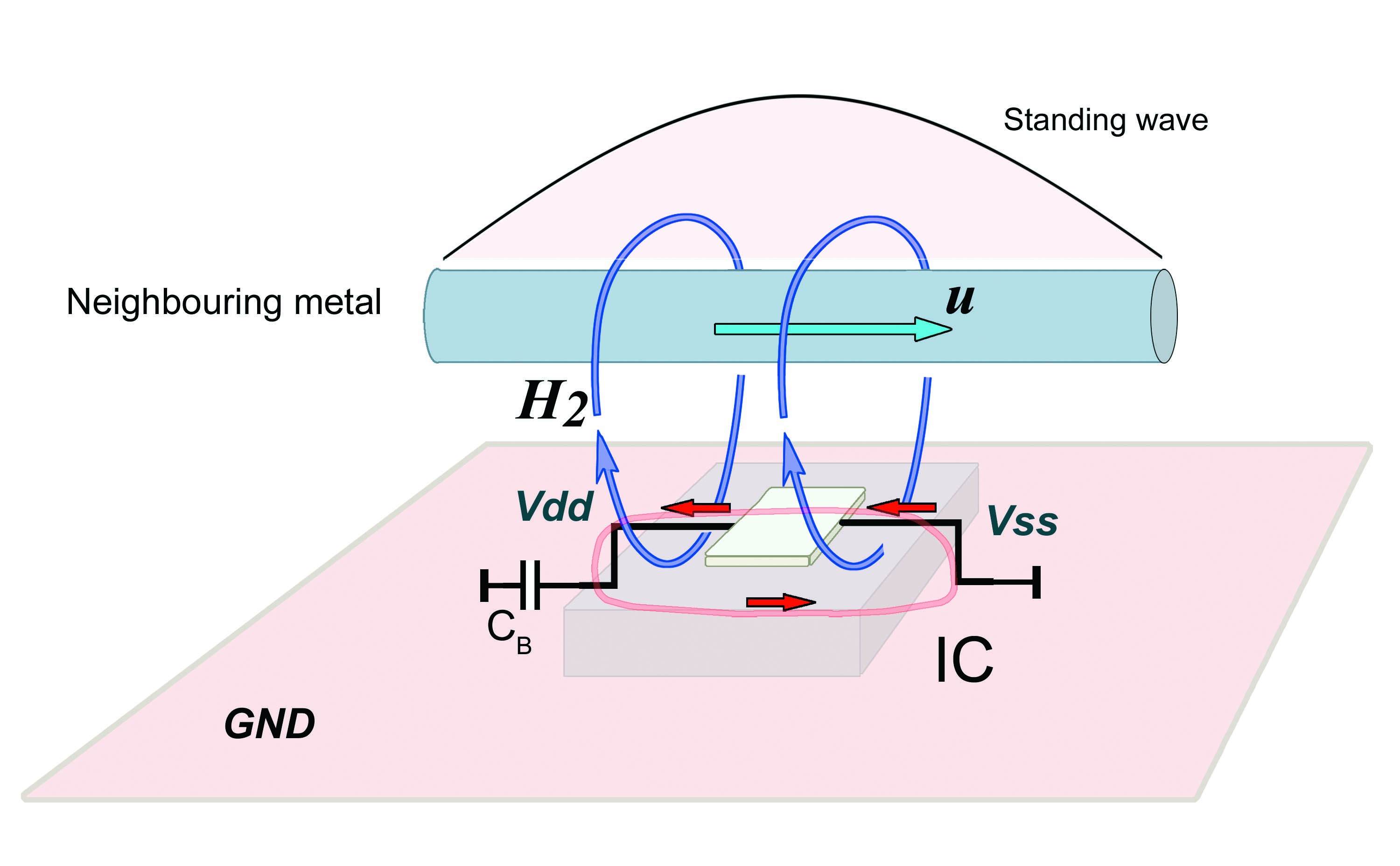
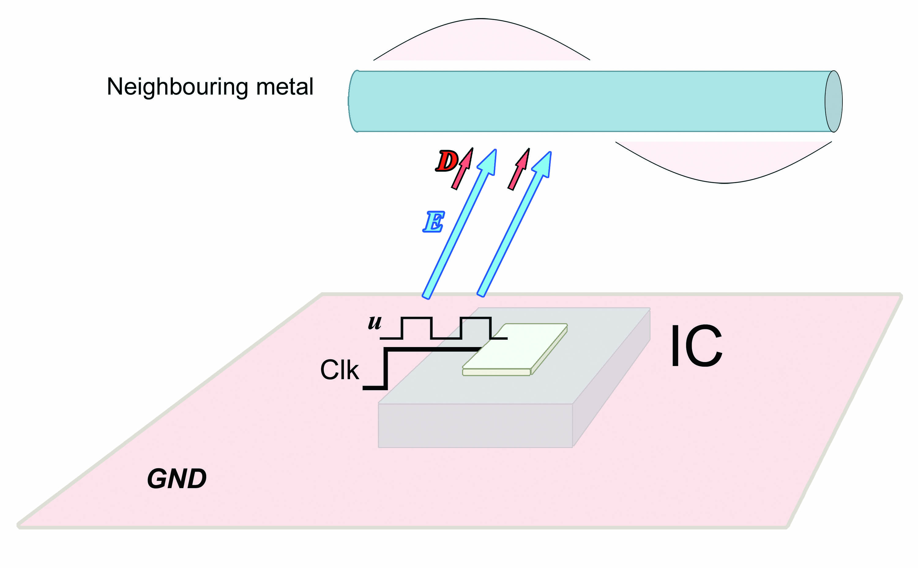
Figure 1 shows a schematic diagram of the coupling mechanisms for both the electric and magnetic fields emerging directly from an IC.
Due to the physical coupling mechanisms, electric fields and associated displacement currents can cause current and/or voltage waves on the PCBs GND system or neighbouring metal parts (Figure 1a).
These metal parts, such as cable harnesses, top-hat rails, etc., act as antennas which are stimulated to emit electromagnetic disturbances through their resonance frequency depending on their spatial dimensions.
The H fields which are generated in the IC (Figure 1b) can also induce a voltage into the PCB’s GND system (H1 field, self-induction) or into neighbouring metal parts (H2 field, counter-induction). This induction voltage will stimulate the metal part to cause emissions in certain frequency ranges.
The developer needs the following information to optimize the IC location and integration in his new circuit:
-
the characteristics of magnetic and electric near fields,
-
the high-frequency currents and voltages on the IC’s inputs and outputs.
TEST METHODS
The following section compares various package alternatives for a microcontroller in terms of different EMC test methods. A controller which is supplied in a 144-pin LQFP and a 144-pin BGA package was chosen for this comparison.
Both types run the same firmware with an identical clock frequency which is generated by external 12 MHz quartz.
The near fields of the ICs were measured on the basis of the TEM cell method (according to IEC 61967-2) on the one hand and with a high-resolution surface scan method (according to IEC 61967-3) on the other. The conducted high-frequency currents and voltages which are coupled out through the pins (measurement according to IEC 61967-4) may also be responsible for disturbance emissions in practice.
Measurement of Conducted High-Frequency Currents and Voltages
This test principle, which is referred to as the 1Ώ/150Ώ direct coupling method in the standard document (IEC 61967-4), is a standard method to measure conducted high-frequency currents and voltages on IC pins. The excitation current is determined with measuring instruments and a 150 Ώ antenna load impedance.
Practical experience has shown that these currents and voltages on the conductor networks in turn generate electrical and magnetic near fields. Maximum emissions are caused by a maximum voltage (generates a maximum E-field) or a maximum current (generates a maximum H-field). It is useful to measure the no-load voltage and short-circuit current directly on the individual pins to determine these disturbances.
The short-circuit current should be determined at a low impedance (<< 1 Ώ) and the no-load voltage at a high impedance (>> 150 Ώ). This helps avoid larger measurement errors due to the IC’s internal impedances for low (under 50 MHz) and high (up to 3 GHz) frequency ranges.
The high-frequency current is deduced from the magnetic field which is measured with probes if a current and voltage measurement on the IC can only be carried out in a specific circuit environment and the measuring equipment cannot be connected due to the high packing density.
No significant magnetic field was measured on the sample IC in the BGA package (Ball Grid Array) since its inputs and outputs were densely packed in ground.
TEM Cell
Today measurements on the basis of the TEM cell are one of the standard assessment methods for disturbance emissions from ICs. With this measuring method the circuit is mounted on a special test board so that the IC is located on one side of the board whereas all other circuit components are on the opposite side. The test board is now fixed in the opening of the TEM cell so that the IC to be tested is inside the measuring chamber and the test board becomes a part of the TEM cell’s wall. The disturbance emissions are measured inside the TEM cell across a so-called septum.
This method does not allow a clear differentiation between electric and magnetic fields. Both fields are always measured together with this method. Depending on the test object’s orientation, voltages which may be generated by both the magnetic and electric fields are thus added or subtracted. Nor does the TEM cell allow any explicit proof of the magnetic excitation field’s orientation, which is another disadvantage. The test board may only be rotated by 90 degrees.
Due to the very wide septum and the large distance to the test object, only a small fraction of the near fields which really exist are measured.
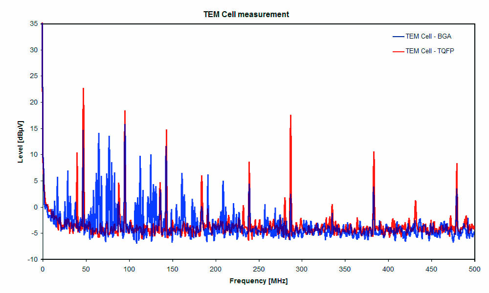
The high-frequency field measurements in the TEM cell showed that the controller in the TQFP package (Thin Quad Flat Pack) had the larger amplitudes as was expected. The large areas and loops which are formed by the controller in this package are a crucial factor in this respect. The 48 MHz core clock and its multiples are clearly visible. They can also be found on the BGA chip which shows much lower measurement levels than the controller in the QFP package.
Measurement of Magnetic and Electric Near Fields
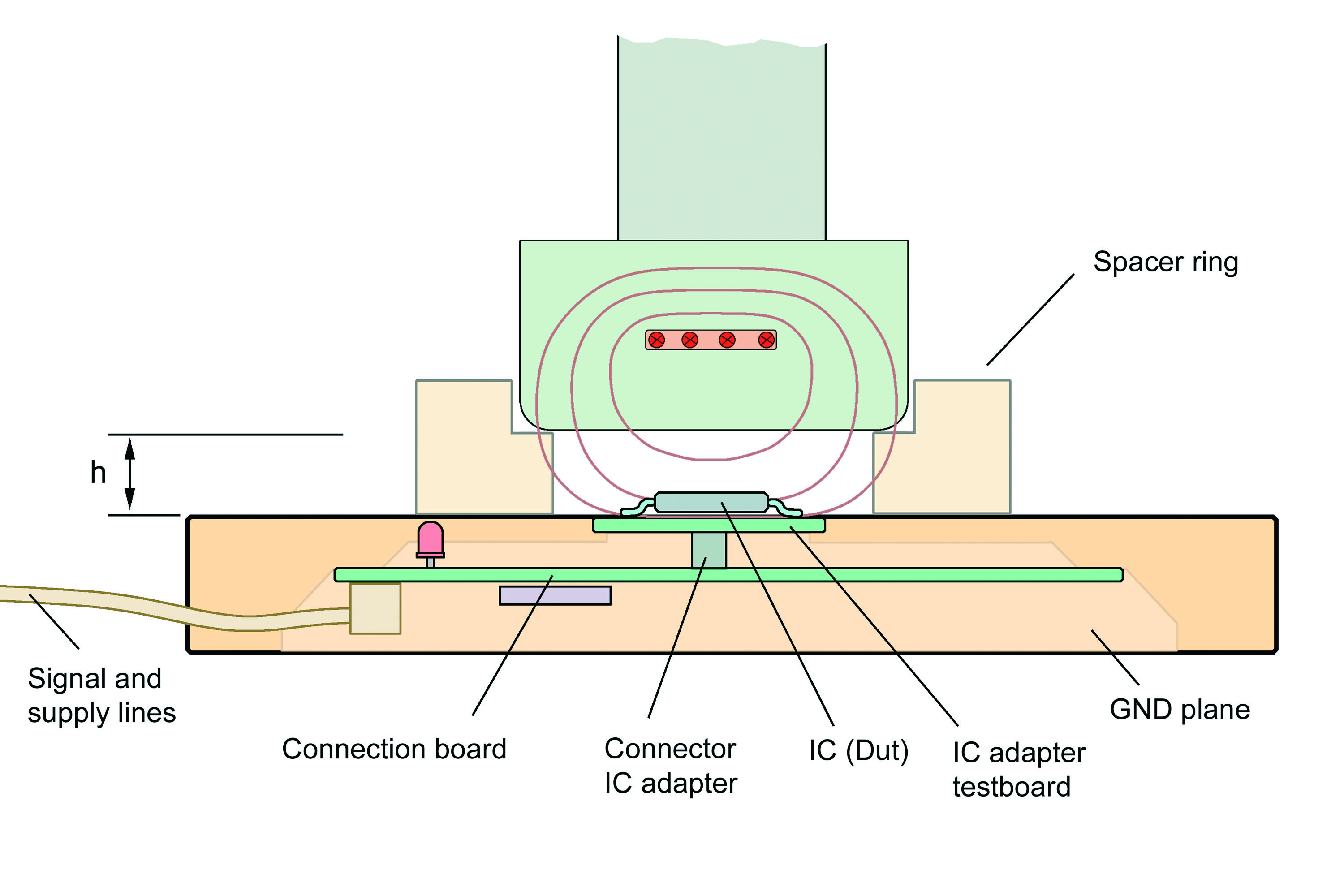
 Magnetic and electric field shares can be differentiated with custom-developed near field probes.
The magnetic fields are measured with a magnetic field loop of 30 mm x 20 mm. This loop’s height and orientation can be varied with the IC package. Magnetic field maxima and minima and consequently the direction of the high-frequency current can thus be determined very precisely.
The electric field shares are detected with a height-adjustable measuring electrode of 25 mm x 25 mm. This is connected to a preamplifier via a very high-impedance input resistor.
Both measurement systems can be used in the frequency range from 16 kHz to 3 GHz. The measurement signal which is internally amplified is displayed on a spectrum analyzer through its 50 Ohm high-frequency measurement output.
Both measuring probes were arranged 10 mm above the GND surface for a comparative measurement of the two package types. The orientation of the H-field loop was matched with that of the septum in the TEM cell in order to be able to directly compare the spectra measured with the TEM cell and near-field probes.
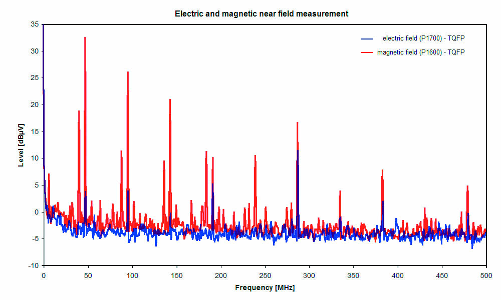
Figure 3 shows some of the measured spectra by way of example: the spectrum measured in the TEM cell on the one hand and the spectra detected with the P1601 probes for magnetic fields and P1701 probes for electric fields on the other.
The physical coupling mechanisms become clearly visible thanks to the differentiation of the near fields with different measuring devices. The peak of the QFP controller at 288 MHz is mainly caused by electric fields whereas the peak of the QFP controller at 240 MHz is almost exclusively produced by magnetic fields.
No electric field could be identified for the BGA controller with the available technology. This is due to the fact that the BGA has a rather compact design and is used in significantly smaller package.
Surface Scan Method
The IC’s local high-frequency sources can be verified for magnetic and electric fields with a very high resolution by a volume or surface scan. The fields resulting from high-frequency currents can be measured above the IC using magnetic-field probes with a different orientation and polarisation.
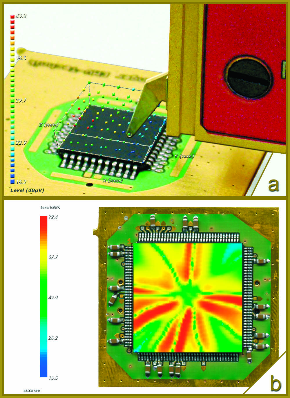
Figure 4a shows a volume scan with a vertical magnetic field probe. The different colours represent the respective magnetic field strength at the measurement points on the different levels. Figure 4b shows the result of a surface scan with a horizontal probe located directly above the IC package.
The frequency shown here is 48 MHz. It can clearly be seen how the 48 MHz core clock is emitted from the IC’s bond wires in the form of a star via the magnetic field. Disturbance emissions may also result if the microcontroller supply is poorly implemented in the application or if a metal conductor is located above the circuit.
SUMMARY AND PROSPECTS
The problems which an IC user has to solve when developing electronic devices and systems are becoming more and more complex. The behaviour of ICs as the source of disturbance emissions cannot yet be fully predicted. But the developer can respond in terms of IC selection or layout planning so that development time and costs can be reduced if the EM characteristics of the ICs used for a new project are already known before the development starts. It is thus necessary to determine the EM characteristics of the circuits to be used in terms of disturbance emissions and immunity before starting the development.
The measurements on the sample ICs clearly show the benefits of the BGA package when it comes to eliminating potentially disturbing emissions from a module. But they also show the necessity of carrying out further physical measurement in addition to the established EMC tests to ensure that the circuits can be put to optimum use in the different modules.
REFERENCES
[1] IEC 61967-1:2002 – Measurement of electromagnetic emissions, 150 kHz to 1 GHz, Part 1: General conditions and definitions
[2] IEC 61967-2:2005 – Measurement of electromagnetic emissions, 150 kHz to 1 GHz, Part 2: Measurement of radiated emissions – TEM cell
[3] IEC 61967-3:2003 – Measurement of electromagnetic emissions, 150 kHz to 1 GHz, Part 3: Measurement of radiated emissions, surface scan method (10 MHz to 3 GHz)
[4] IEC 61967-4:2002 – Measurement of electromagnetic emissions, 150 kHz to 1 GHz, Part 4: Measurement of conducted emissions – 1 ohm/150 ohm direct coupling method
ABOUT THE AUTHOR
Sven König is responsible for the tests and measurement equipment for electronic semiconductors at Langer EMV-Technik GmbH in Bannewitz. König was born in Dresden and studied electrical engineering at the “Studienakademie” in Bautzen. He has been an engineer at the Langer EMV-Technik GmbH since 2007.
