Bruce Archambeault, Ph. D.
IBM
Research Triangle Park, NC
Barch@us.ibm.com
Introduction
The use of decoupling capacitors connected between the power and ground planes on a printed circuit board (PCB) is a common practice to help ensure proper functionality and to reduce EMI emissions from printed circuit boards. The proper number of decoupling capacitors, and the proper value of those decoupling capacitors is always a topic of debate between EMC engineers and design engineers. Some typical rules-of-thumb require a decoupling capacitor for each power pin on an IC. Other rules-of-thumb require at least one decoupling capacitor per side of physically large ICs. Still other rules-of-thumb require decoupling capacitors spread evenly over every square inch of the board. Very little real information about the optimum approach is available in the technical literature. These rules of thumb result in a drastic over design of the decoupling strategy, since the saying ‘better safe than sorry’ is usually applied. Many of these rules-of-thumb are really based in a myth. In addition to these rules-of-thumb, there are a number of outright myths that exist and are published, adding significant confusion to the general design community. Some of these myths have some amount of rational to justify them, others do not. One recent myth claimed that the decoupling capacitors actually caused the emissions! However, most myths are not so easy to discount.
Traditionally, the values of the decoupling capacitors are largely based upon habit and the experience of the EMC engineer. Values of 0.01 uf or 0.1 uF are typically used. Often smaller capacitors are used in parallel with the main decoupling capacitor to provide a high frequency and a low frequency filtering effect. However, potential cross resonances can have a negative effect when using multiple capacitors in close proximity.
The overall result is that the design of the power plane decoupling (between a power plane and a ground reference plane) has been historically difficult to properly design or analyze. With on-board clock speeds of 400 – 800 MHz becoming common, a more rational approach must be taken to optimize the design of decoupling capacitors on the printed circuit (PC) board.
Background
There are two primary purposes for using decoupling between power and ground-reference planes. The first purpose is for functionality, that is, the decoupling capacitor is a charge storage device, and when the IC switches state and requires additional current, the local decoupling capacitor supplies this current through a low inductance path. If the capacitor is able to supply all of the current required by the IC, then the voltage remains constant (whatever the supply voltage is set to be). If the capacitor is not able to supply the required current, then the voltage at the IC power pin is lowered temporarily until enough current is provided, or until the need for the current is ended. If enough current is not provided, the IC may have a functional failure. Therefore, it is important to locate decoupling capacitors close to the demand for current (IC power pins, and to have a low inductance path from the IC power pins to the power plane, and from the IC’s ground-reference pins to the ground-reference plane, and from the decoupling capacitor to the power and ground-reference planes.
The second purpose for decoupling capacitors is to reduce the noise injected into the power and ground-reference plane pairs and thus reduce the EMI emissions from the edge of the circuit board. The edge of a board may be near the seams of the metal enclosure, or near an air vent area, allowing this noise to escape the enclosure. Another possibility is for this noise to couple onto I/O connector pins, and be directly coupled out of the metal enclosure on the cables, etc.
The source of this noise is one of two causes: (1) the temporary lowering of voltage at the IC pin power pin when sufficient current is not provided from the decoupling capacitor (a short duration voltage pulse), or (2) the noise signal injected between the power and ground-reference planes due to an intentional current on a via with the clock signal or other fast switching signal. It has been shown by measurements on active ICs that the relative size of these two causes of noise between typical power and ground-reference planes is about the same.
Once a signal from either source results in noise between the power and ground-reference planes, the goal is to reduce the noise voltage level using decoupling capacitors.
Decoupling Capacitor Performance Measurement Process
Since a ‘real’ PC board is quite complex, it is difficult to isolate the various EMC effects to know that a particular change to the board has produced an effect that is directly traceable to that original change. Therefore, a special PC board was created to help analyze the effects of a variety of decoupling capacitor configurations.
Test Board Description
This investigation focused upon a 4-layer PC board, with the external dimensions of 10 x 12 inches. This was considered to be a typical board used in current products. Since the frequency range under investigation extended from 30 MHz to over 1 GHz, a repeatable and well controlled connection method to the test board was required. A set of 15 SMA connectors were installed across the board as shown in Figure 1. Each of the SMA connectors was surrounded by four locations for SMT decoupling capacitors. Figure 2 shows the detail of each location.
Figure 1-Test Board SMA Connector Configuration
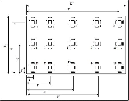
Figure 2 -Test Board SMA Connector Area Detail
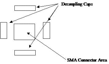
Figure 3- Additional Decoupling Capacitor Locations on Test Board
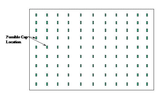
In addition to the SMA connectors, and the surrounding decoupling capacitor sites, locations for additional SMT decoupling capacitors were located every inch on the PC board. Figure 3 shows a diagram of the additional decoupling capacitor locations.
All measurements were taken with a Network/Impedance analyzer. Both one-port and two-port measurements were used. One port measurements were impedance measurements, while the two port measurements were S21[1]. Examples of each result will be provided in the following section.
Initial measurements were impedance measurements. Observing the impedance across the frequency range of 30 – 1800 MHz allowed a better understanding of the effectiveness of the natural interplane capacitance, the effects of decoupling capacitors, and board resonances. However, impedance at a given location on a PC board is not the primary concern for EMC engineers. A more important parameter for EMC engineers is the amount of ‘noise’[2] at a remote location due to some IC source location. The remote location might be the edge of the PC board (where it was located near a seam in the metal shielded enclosure), or near a via for an I/O signal trace, which was then connected to an external connector. Therefore, the S21 parameter is a better indication of the decoupling configuration’s performance for EMC considerations. The goal is to have as low as possible S21 between a potential source, and a remote location of concern.
Decoupling Capacitor Configuration Measurement Results
There was a number of different types of decoupling configurations measured, as well as the capacitor value being varied. The difference between local source decoupling, and distributed decoupling was then investigated. Finally, the number of capacitors, and various values of capacitance (both single and multiple values) were investigated.
Throughout the measurements of the S21 transfer function, significant resonant effects were noticed at high frequencies. Above 200 MHz, resonances due to the board dimensions become the dominant factor. Depending upon which location on the PC board was used for the transfer function measurement, a particular resonant frequency might be excited, or might not be excited. However, from an EMC point of view, it is not possible to control where a component might be placed so to ensure a particular resonance mode would not be excited, so all modes must be assumed present. For this set of experiments, the center and one corner port were used so that most of the resonant modes would be excited over the frequency range of interest (< 2 GHz).
Further experiments with various capacitor values at various locations showed that while a particular resonant frequency would shift to another frequency (as capacitors were added and/or moved about the board), the general shape and level of impedance of the resonant peaks did not change. This indicates that the entire resonant frequency range must be considered resonant. That is, since the frequency of resonance shift with any changes, then all frequencies must be assumed to be resonant, and the overall envelope of the S21 transfer function lowered. These resonances are extremely important, and require a full wave analysis to consider the physical dimensions of the board. This makes SPICE circuit analysis ineffective for high frequency decoupling analysis.
Source Vs Distributed Decoupling
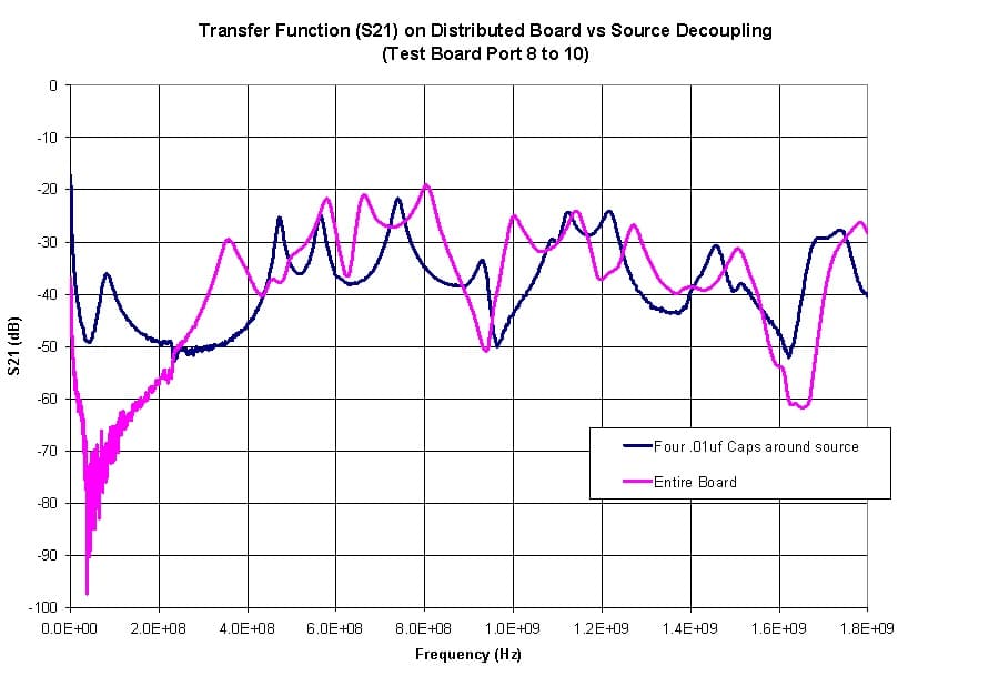
As mentioned earlier, a common question amongst EMC and design engineers is whether to place decoupling capacitors close to the source of the ‘noise’ (that is, near the power and/or ground pins of the ICs), or to simply distribute them across the entire board. To help determine the best design approach, the S21 transfer function of the test PC board were measured with no capacitors, and then with four 0.01 uF capacitors only around the source SMA connector and within 100 mils, and then with 0.01 uF capacitors distributed across the entire board.
Figure 4 shows the S21 results between ports 8 and 10 on the test PC board. Note that the scales have been changed to better display the S21 data, and that a log (dB) scale is used for S21 amplitude[3]. The results showed that the only difference between the no-capacitor case and the four-close-to-the-source-capacitor case was below about 50 MHz. Figure 4 also shows very little improvement[4] was observed at frequencies above 200 MHz even with the board fully populated with capacitors. This is due to the impedance of the .01uf capacitor SMT capacitor being greatly affected by it’s internal inductance (and the inductance of the pads and vias on the board).
While a distributed decoupling strategy appears to be best for an EMC design, signal integrity design considerations still require a decoupling capacitor near a high speed IC to provide the necessary supply current with as low series inductance as possible. A combination of decoupling strategies will meet both EMC and signal integrity requirements.
Figure 4
Quantity of Distributed Decoupling Capacitors (.01uf Only)
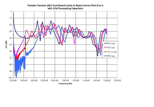
The investigation into the number of decoupling capacitors distributed across the board used only 0.01 uF SMT [5] capacitors. The S21 ‘transfer function’ was measured for a variety of different port combinations, and with a variety of capacitors distributed across the board. Every effort was made to distribute the capacitors evenly across the board for all quantities of capacitors. The results and conclusions for the various board source and receive locations was consistent. While the individual resonances might shift slightly, the overall envelope of the S21 transfer function was not affected by location. Therefore, only one source and receive pair will be reported here.
As can be seen in Figure 5, adding capacitors lowered the S21 transfer function in the lower frequency ranges (below 200 – 400 MHz). Also, at higher frequencies, the overall envelop for the S21 transfer function decreased only very slightly (even though the resonant frequency shifted) as more capacitors were added.
The maximum number of capacitors was 99 distributed capacitors, representing one capacitor every square inch across the PC test board. This is a much denser capacitor placement than is likely to be acceptable on real products.
Figure 5
Quantity of Distributed Decoupling Capacitors (0.01uf and 330pf)
There has recently been a lot of discussion about using a combination of so-called high-frequency capacitors and regular capacitors to try to ‘tune’ the decoupling performance over a wide range of frequencies. Most of this analysis is performed using SPICE circuit type analysis, which ignores the three dimensional full wave nature of PC boards.
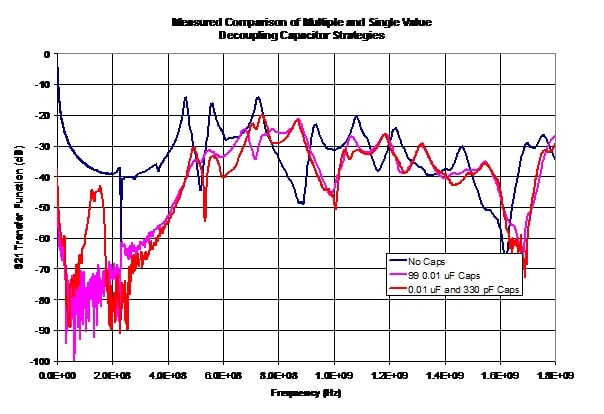
The 0.01 uF capacitors were combined with 330 pF capacitors to determine the effect on the high frequency performance of S21 when two different values of capacitors were used. For this set of experiments, the test PC board was completely populated with alternating .01 uf and 330 pF capacitors (all 99 locations had a .01 uF capacitor or a 330 pF capacitor, but not both values). This set of experiments was again repeated for a number of different port-to-port combinations and a variety of different capacitor values. The results from the various combinations were again consistent, and only one result is shown here.
The results in Figure 6 show that at frequencies below about 75 MHz, the S21 behavior is very similar to the case with only 0.01 uF capacitors. However, the S21 transfer function is dramatically worse in the 75 – 200 MHz range due to cross resonances (the capacitance of one capacitor resonates with the inductance of the other capacitor and the inductance of the planes between them). There is no noticeable improvement of the high frequency decoupling performance with the addition of the second value of capacitance. In fact, the over all decoupling performance is worse in a frequency range where much of the typical noise energy exists (50 – 200 MHz).
Figure 6
Selecting the Value of the Decoupling Capacitors
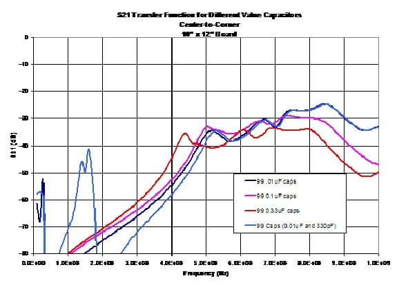
The actual value of the decoupling capacitors is another topic for hot debate. A series of experiments were performed to show the effects of different capacitor values. The results are shown in Figure 7.
The capacitor value was changed from 0.01 uF to 0.1 uF and 0.33 uF without a significant change in the high frequency performance of the transfer function. Again, the inductance of the capacitor and the vias overwhelms the impedance of the capacitor at high frequencies. The optimum solution is to pick a SMT capacitor size, and then use the largest value of capacitance available in that package size.
Lossy Capacitors
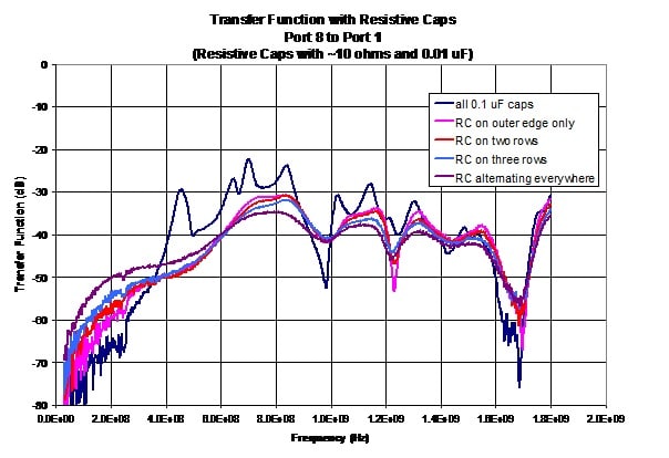
It is commonly accepted that decoupling capacitors should have low equivalent series resistance (ESR). However, it has been shown that at high frequencies, normal circuit type analogies are not consistent with the measured results, and that the physical resonances of the board dominate at high frequencies. Therefore, it is necessary to add some amount of loss to dampen the Q factor of these resonances. A series of experiments with high ESR capacitors (about 10 ohms in series with a 0.1 uF capacitor in the same SMT package) showed that lossy capacitors can have a significant effect at high frequencies. Figure 8 shows the results from these measurement. The best case seems to be when about 50% of the total capacitors are lossy and the remaining 50% are regular low ESR capacitors.
Figure 8
Summary
Careful measurements have shown that many of the common decoupling myths are false. While many of these myths are considered ‘rules of thumb’, they have no basis in a science which includes all the real-world and full wave three dimensional effects. The proper decoupling strategy for PC boards need to account for the two purposes of these capacitors. In order to provide rapid charge delivery to the IC for functionality, a low ESR capacitor should be placed close to the IC’s power and ground pins. However, this does little or nothing for the EMC problem.
The EMC problem requires that a distributed capacitor strategy be used. That is, the capacitors should be distributed over the entire board. This is not inconsistent with the functionality requirement, since a capacitor near an IC can serve both purposes easily.
It has also been shown that the actual value of the capacitor is not important. It is recommended that the largest value of capacitance within the selected surface mount package size be used.
It has been shown that a single value of capacitance is better than multiple values. The multiple values do not help at high frequencies (because of the inductance of the vias, etc.), and can actually decrease the decoupling performance significantly at lower frequencies. The decreased decoupling performance is due to unavoidable cross resonances between components.
And finally, it was shown that lossy, or ‘high ESR’ capacitors can actually improve the decoupling performance at high frequencies. These lossy capacitors should be used in combination with normal capacitors.
It is hoped that this systematic approach to decoupling design strategy will help engineers understand the trade-offs associated with the various options. It is further hoped that engineers are now better able to discount the many myths and misconceptions that abound.
Footnotes
[1]S21 is a measure of the ratio of output voltage to the input voltage.
[2] The noise in this case is due to either the switching within the IC, and the current drawn from the power/ground plane structure to support the sudden switching, or from a critical net making a layer transition through a via.
[3] If S21 is equal to one, or zero dB, that would indicate that all the source voltage was present at the remote observation point.
[4] From an EMC point of view, a lower S21 result is a ‘better’ result.
[5] Surface mount style capacitors in the 0805 package size was used throughout this study.


