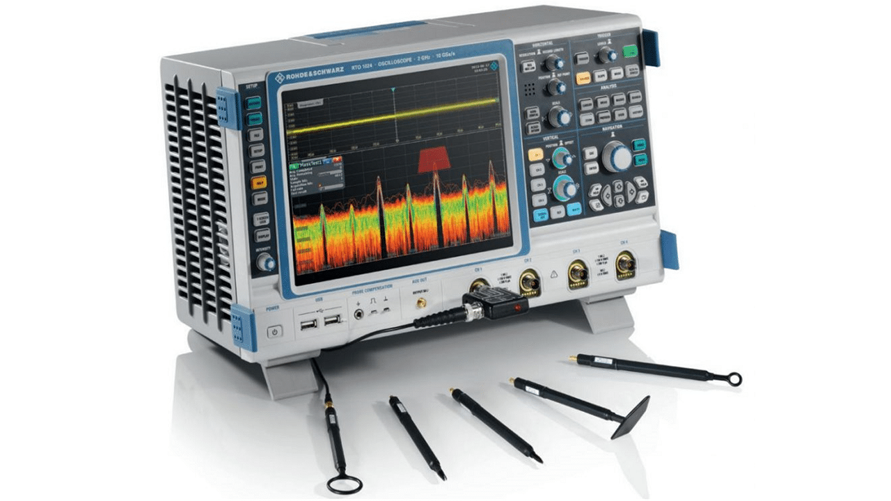
This month, I will explain one of the most useful functions you can find in the Rohde & Schwarz RTO family of digital scopes (Fig. 1): the FFT gating function. This is a function I like to use in the demonstrations included in many of my courses and seminars.
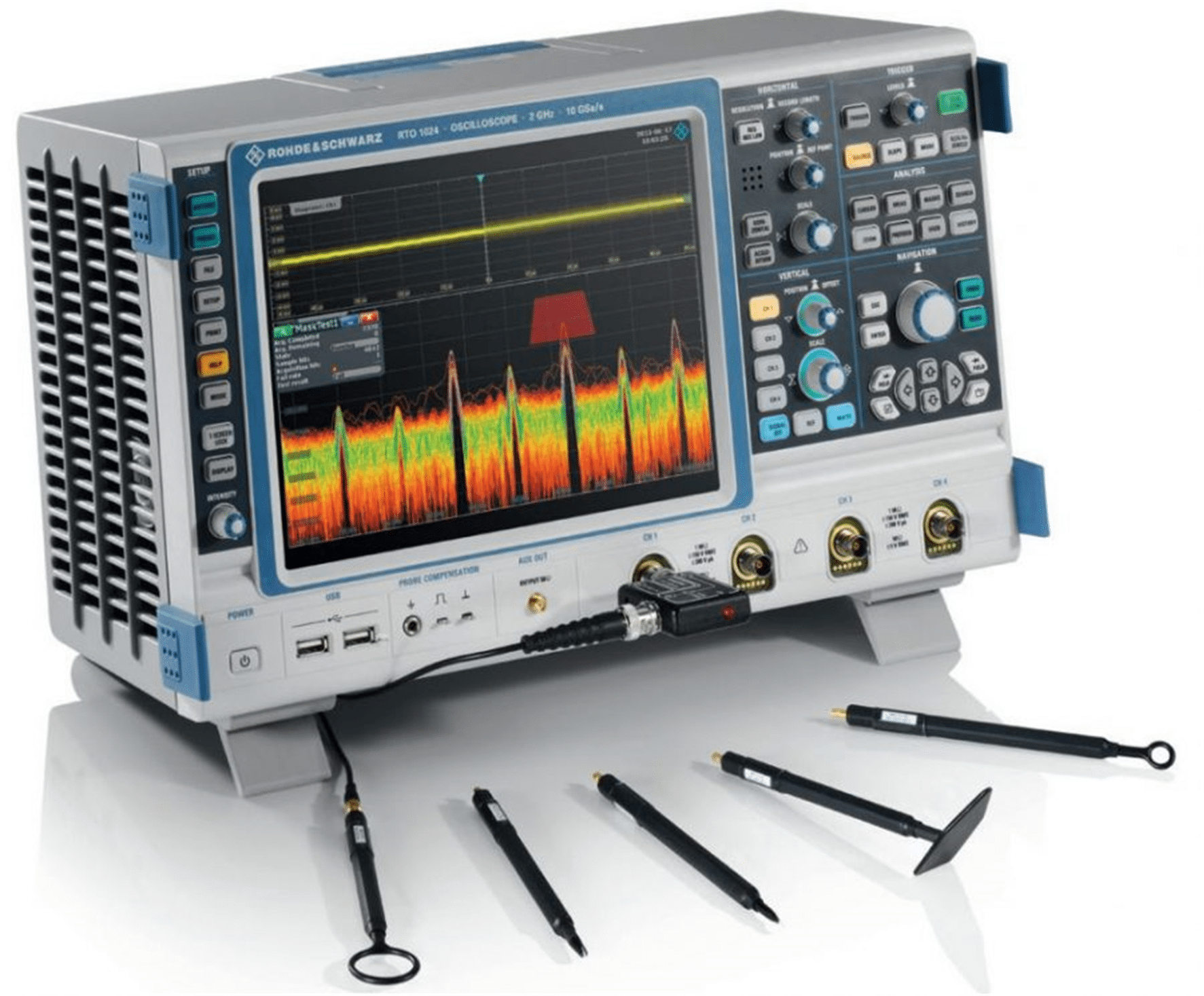
Fig. 1. An RTO digital scope (photo courtesy R&S]
The RTO family of digital scopes is ideal for EMI troubleshooting because they offer: high sensitivity (1 mV/div), high bandwidth (up to 6 GHz at this moment), very low input noise, an incredibly powerful FFT, four channels, and many other special characteristics.
Fours channels are really useful, in my opinion, because you can to combine:
- voltage probes (passive and active),
- current probes (for measuring differential and common mode EMI currents),
- near field probes (both electric and magnetic probes),
- antennas (for measuring in the far field),
- and line impedance stabilization networks (LISN) for conducted emissions in DC or AC power supplies.
And for all those probes I like to combine both the time and frequency domains for a complete analysis of EMI/EMC problems.
In state of the art scopes, we can find really great FFT capabilities associated to specific hardware per channel with high acquisition bandwidth.
Do you remember the first scopes with FFT capabilities?
They were really difficult (non-intuitive tools) to configure because frequency range and span were controlled by the time domain settings.
Setting up the FFT in RTOs is EASY (Fig. 2). It is configured in a similar way to traditional spectrum analyzers with START-STOP frequencies, or CENTER FREQUENCY-SPAN, and RBW (resolution bandwidth).
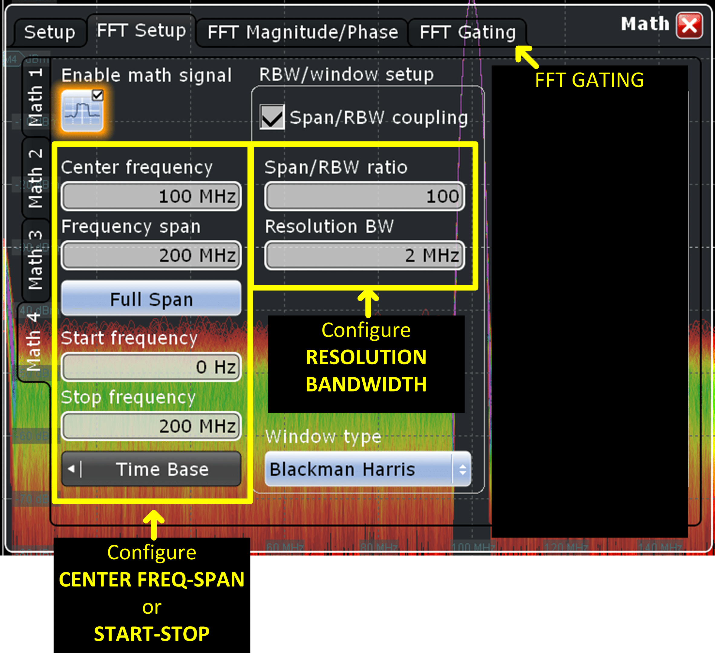
Fig. 2. How to configure the FFT for the frequency range of interest.
Choose your desired values and the scope automatically configures the time domain capture to offer the desired frequency spectrum analysis.
In the FFT menu you can enable the FFT gating function so you will be able to correlate sporadic emissions with events in the time domain.
With “Gated FFT” you are able to calculate the FFT for a specific interval in the acquired time domain signal.
Consider for example, you are designing a product with a DC/DC (buck) converter. As many of you know, DC/DC converters are aggressive systems because their switching nature. They can create serious conducted and radiated problems.
In our example, we have a product represented as in Fig. 3.
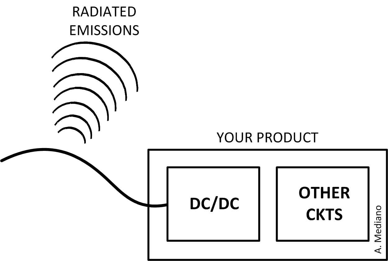
Fig. 3. The system is failing in radiated emissions.
The product was failing in radiated emissions in the VHF range and the power supply cable was the culprit antenna.
Note the cable is radiating because the it is being excited with common mode (CM) currents. And remember that as low as 10-15uA of CM current in your cables can be the origin of failing in radiated emissions in a typical radiated emissions test at 3 meters.
Let’s check the common mode current in both time and frequency domain using a current probe as in Fig. 4.
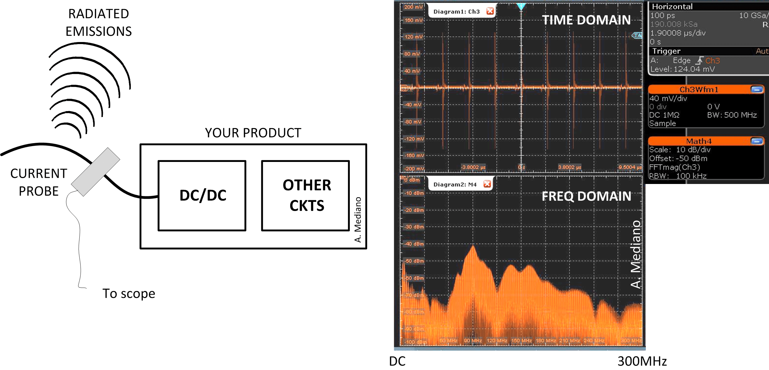
Fig. 4. Measuring CM current in a cable of our system.
Where is the origin of that signal?
We used a near field probe to locate the signal. After sniffing around the full product we located the source on top of the DC/DC converter, and especially over the output diode (Fig. 5).
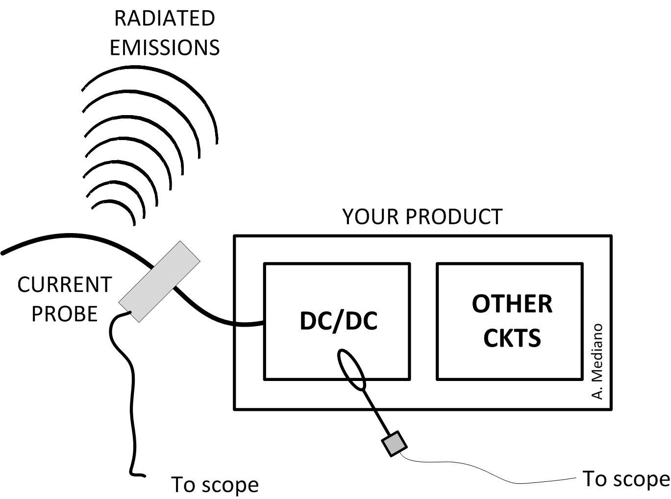
Fig. 5. Measuring CM current in a cable with a near field probe on top of the buck converter diode.
In Fig. 6, the left traces are common mode current in cable from DC to 300 MHz as from previous figure. The output of the near field probe (NFP) is in the traces on the right. Signals are shown in different colors and in time and frequency domains.
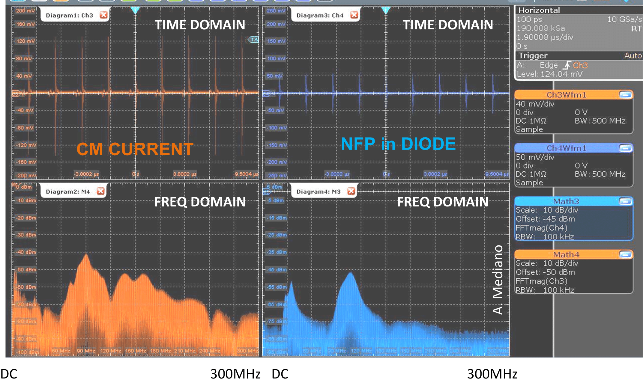
Fig. 6. Measuring CM current in cable and field on top of the diode.
The peak in our VHF range of interest is related with the ringing in the diode. A different diode, layout, or adding a ferrite bead, etc. are typical solutions to this problem.
For our example, the time domain signal is simple but in other applications the signal is very complicated or difficult to analyze.
Is it possible for those simple or complex time domain waveforms to know in what part of the time domain signal the RF energy is created? That information could be very useful to understand how our circuit is generating EMI. The answer to this question is the Gated FFT function.
Let’s activate the FTT gating using our previous example (Fig. 7).
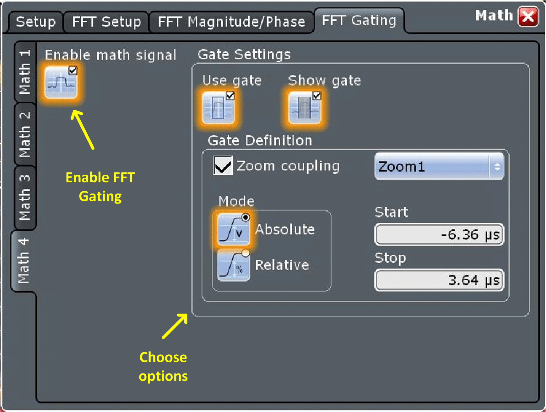
Fig. 7. Menu for activating FFT Gating.
A time window (gate) appears highlighted in gray (Fig. 8).
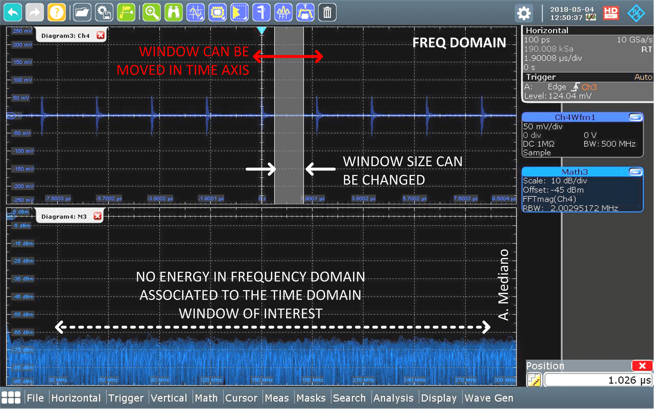
Fig. 8. NFP signal with FFT gating with window in a time domain section where no RF energy is created.
In Fig. 8 the window is located between two of the transients of the near field output. Note FFT display shows there is no energy in that frequency range.

Fig. 8. In between switching transients, there is no RF energy measured.
The window can be moved (red arrows) across the entire acquisition period so we can determine what segments of the time domain signal correlate with the frequencies where we are failing in EMC tests. The window can additionally change width (white arrows). Those limits and position can be established with the control knob in Fig. 9 or using the tactile capabilities of the screen.
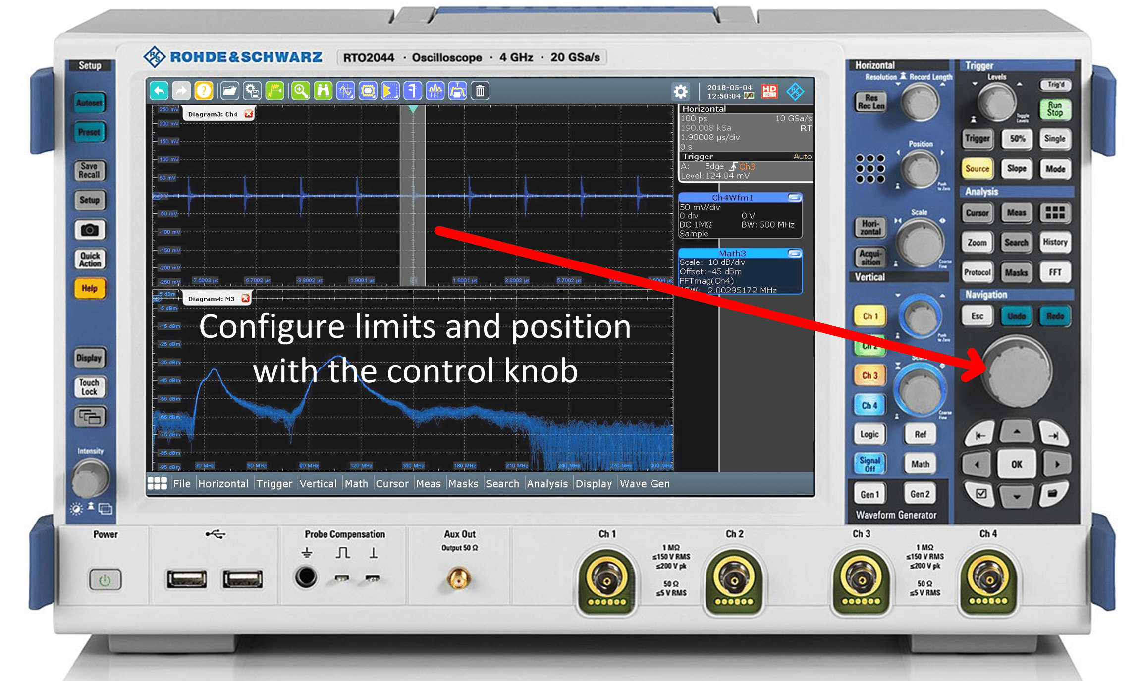
Fig. 9. The knob control to configure the limits and position for the FFT gating window.
In Fig. 10 the gating window displays the ringing on top of the diode and, in real time we see the RF energy in the FFT screen.
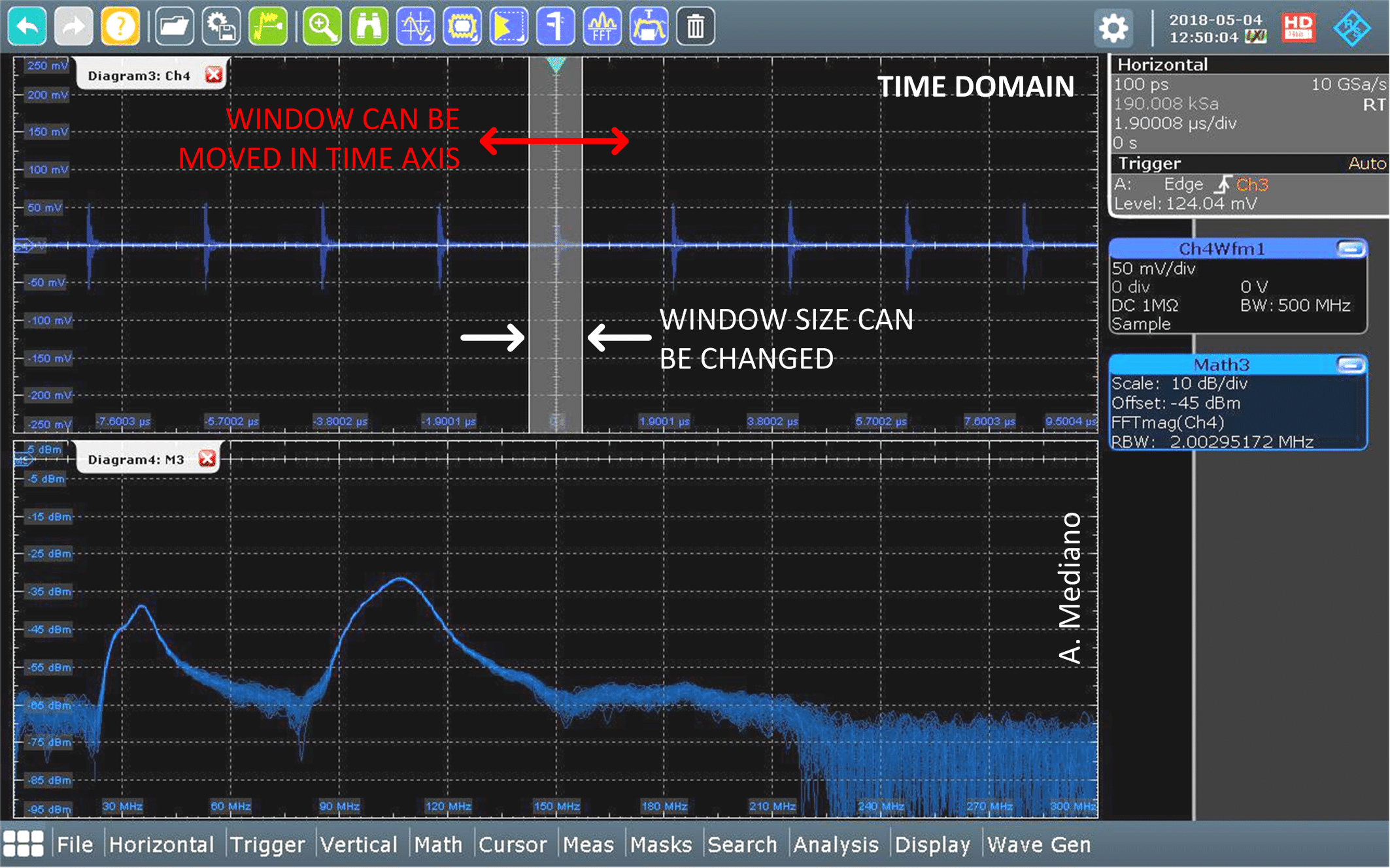
Fig. 10. NFP signal with FFT gating with window in a time domain section where RF energy is created.
The possibilities of combining FFT gating with four signals (channels), and in time and frequency domains are only limited by our minds. With the good information on screen we can quickly assess the effectiveness of countermeasures: ferrites, capacitors, changes in layout, alternative components, etc.
As usual, if you can see your problem on screen you will be able to solve your problems more easily.
