Introduction
While unrealistic to discuss all aspects of product design in a single article, I’ll try to describe the most common design issues I find in the hundreds of client products I’ve had a chance to work on. These issues generally include PC board design, cables, shielding, and filtering. More detailed information may be found in the Reference section below.
As previously mentioned, the top three product failures I run into include (1) radiated emissions, (2) radiated susceptibility, and (3) electrostatic discharge. Other failures can include things like conducted emissions, electrically fast transient, conducted susceptibility, and electrical surge. Most of these last items are also the result of the same poor product designs, which cause the top three failures.
PC Board Design
The single most important factor in achieving EMC/EMI compliance revolves around the printed circuit board design. It’s important to note that not all information sources (books, magazine articles, or manufacturer’s application notes) are correct when it comes to designing PC boards for EMC compliance – especially sources older than 10 years, or so. In addition, many “rules of thumb” are based on specific designs, which may not apply to future or leveraged designs. Some rules of thumb were just plain lucky to have worked.
PC boards must be designed from a physics point of view and the most important consideration is that high frequency signals, clocks, and power distribution networks (PDNs) must be designed as transmission lines. This means that the signal or energy transferred is propagated as an electromagnetic wave. PDNs are a special case, as they must carry both DC current and be able to supply energy for switching transients with minimal simultaneous switching noise (SSN). The characteristic impedance of PDNs is designed with very low impedance (0.1 to 1.0 Ohms, typically). Signal traces, on the other hand, are usually designed with a characteristic impedance of 50 to 100 Ohms.
The previous article introduced the concept of the circuit theory and field theory viewpoints. A successful PC board design accounts for both viewpoints. Circuit theory suggests that current flows in loops from source to load and back to the source. In many cases of product failure, the return path has not been well defined and in some cases, the path is broken. Breaks or gaps in the return path are major causes of radiated emissions, radiated susceptibility, and ESD failures.
Correspondingly, electric fields on PC boards exist between two pieces of metal, such as a microstrip over a return plane (or trace). If the return path is broken, the electric field will “latch on” to the next closest metal and will not likely be the return path you want. When the return path is undefined, then the electromagnetic field will “leak” throughout the dielectric and cause common mode currents to flow all over the board, as well as cause cross-coupling of clocks or other high speed signals to dozens of other circuit traces within that same dielectric.
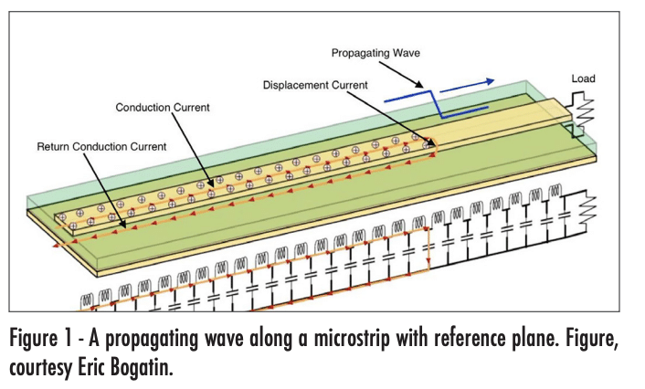
Figure 1 shows a propagating wave within the dielectric between the signal trace and return plane (or trace). This shows both the conduction current flowing in the signal trace and back on the return plane (or trace) and the displacement current “through” the dielectric. The signal wave front travels at some fraction of the speed of light as determined by the dielectric constant. In air, signals travel at about 12 inches per nanosecond. In the typical FR4 dielectric, the speed is about half that at 6 inches per nanosecond. Refer to Reference 1, 2, and 3 for more information on the physics of signal propagation through PC boards.
In order to satisfy both the circuit and field theory viewpoints, we now see the importance of adjacent power and power return planes, as well as adjacent signal and signal return planes. PDN design also requires both bulk and decoupling “energy storage” capacitors. The bulk capacitors 4.7 to 10 μF, typ.) are usually placed near the power input connector and the decoupling capacitors (1 to 10 nF, typ) nearest the noisiest switching devices – and most importantly, with minimal trace length connecting these from the power pins to signal return plane. Ideally, all decoupling capacitors should be mounted right over (or close to) the connecting vias and multiple vias should be used for each capacitor to reduce series inductance.
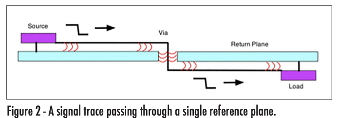
Signal or power routed referenced to a single plane will always have a defined return path back to the source. Figure 2 shows how the electromagnetic field stays within the dielectric on both sides of the return plane. The dielectric is not shown for clarity.
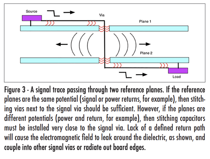
On the other hand, referring to Figure 3, if a signal passes through two reference planes, things get a lot trickier. If the two planes are the same potential (for example, both are return planes), then simple connecting vias may be added adjacent to the signal via. These will form a nice defined return path back to the source.
If the two planes are differing potentials (for example, power and return), then stitching capacitors must be placed adjacent to the signal via. Lack of a defined return path will cause the electromagnetic wave to propagate throughout the dielectric, causing cross coupling to other signal vias and leakage and radiation out the board edges as shown.
For example, let’s take a look at a poor (but very typical) board stack-up that I see often. See Figure 4.
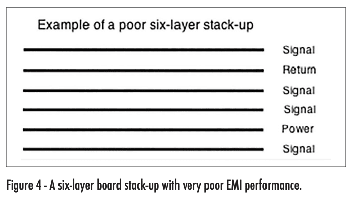
Notice the power and power return planes are three layers apart. Any PDN transients will tend to cross couple to the two signal layers in between. Similarly, few of the signal layers have an adjacent return plane, therefore, the propagating wave return path will jump all over to whatever is the closest metal on the way back to the source. Again, this will tend to couple clock noise throughout the board.
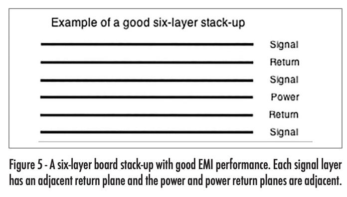
A better design is shown in Figure 5. Here, we lose one signal layer, but we see the power and power return planes are adjacent, while each signal layer has an adjacent signal (or power) return plane. It’s also a good idea to run multiple connecting vias between the two return planes in order to guarantee the lowest impedance path back to the source. The EMI performance will be significantly improved using this, or similar designs. In many cases, simply rearranging the stack-up is enough to pass emissions.
Note that when running signals between the top and bottom layers, you’ll need to include “stitching” vias between the return planes and stitching capacitors between the power and power return planes right at the point of signal penetration in order to minimize the return path. Ideally, these stitching vias should be located within 1 to 2 mm of each signal via.
Other Tips – Other design tips include placement of all power and I/O connectors along one edge of the board. This tends to reduce the high frequency voltage drop between connectors, thus minimizing cable radiation. Also, segregation of digital, analog, and RF circuits is a good idea, because this minimizes cross coupling between noisy and sensitive circuitry.
Of course, high-speed clocks, or similar high-speed signals, should be run in as short and as direct a path as possible. These fast signals should not be run long board edges or pass near connectors.
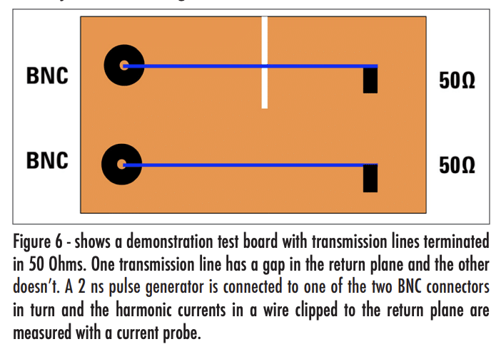
Gaps in Return Plane – I’d like to come back to the gap or slot in the return plane mentioned earlier and show an example of why it’s bad news for EMI. When the return path is interrupted, the conduction current is forced around the slot, or otherwise finds the nearest (lowest impedance) path back to the source. The electromagnetic field is forced out and the field will “leak” all over the board. I have an article and good demonstration video of this and how it affects common mode currents and ultimately, EMI. See Figure 6 and Reference 4.
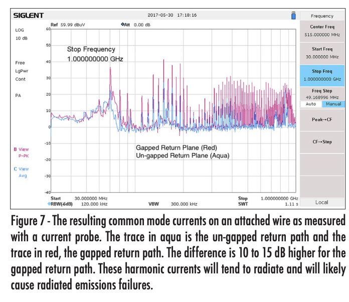
The difference between the gapped and un-gapped traces is shown in Figure 7. Note the harmonic currents are 10 to 15 dB higher for the gapped trace (in red). Failing to pay attention to the signal and power return paths is a major cause of radiated emissions failures.
Shielding
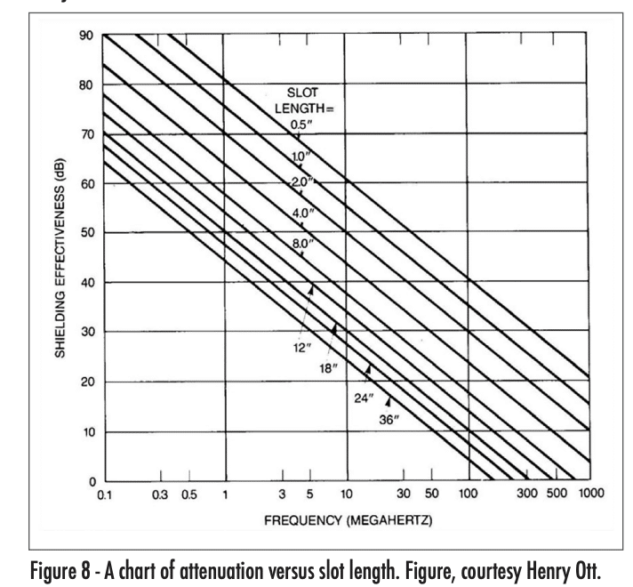
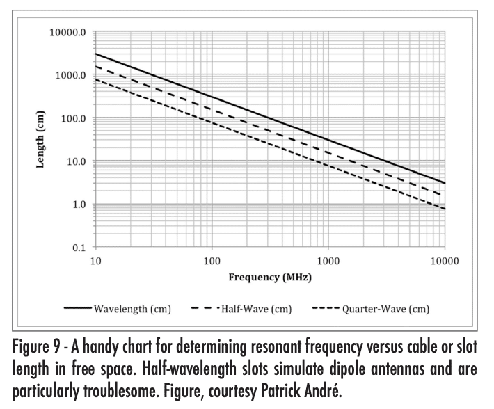
The two issues with shielded enclosures is getting all pieces well-bonded to each other and to allow power or I/O cable to penetrate it without causing leakage of common mode currents. Bonding between sheet metal may require EMI gaskets or other bonding techniques. Slots or apertures in shielded enclosures become issues when the longest dimension approaches a half wavelength. Figure 8 shows a handy chart for determining the 20 dB attenuation of a given slot length. See Reference 5 and 6 for more detail on shielding. Interference Technology also has a free downloadable 2016 EMI Shielding Guide with excellent information (Reference 7).
Figure 9 is a chart of wavelength versus frequency. For example a 6-inch (15 cm) slot has a half wave resonance at 1000 MHz. If a product design requires at least a 20 dB shielding effectiveness, then the longest slot length can be just one-half inch.
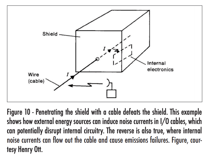
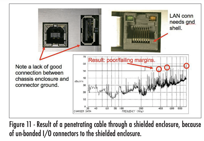
Cable Penetration – The number one issue I find when tracking down a radiated emissions problem is cable radiation. The reason cables radiate is that they penetrate a shielded enclosure without some sort of treatment – either bonding the cable shield to the metal enclosure or common mode filtering at the I/O or power connector (Figure 10 and 11). This occurs frequently, because most connectors are attached directly to the circuit board and are then poked through holes in the shield. Once the cable is plugged in, it is “penetrating the shield” and EMI is the usual result.
There are four combinations or cases that must be considered: shielded or unshielded products, and shielded or unshielded cables. Power cables are usually unshielded for consumer/commercial products and so require power line filtering at the point of penetration or at the connector of the circuit board. Shielded cables must have the shield bonded (ideally in a 360 degree connection) to the product’s shielded enclosure. If the product does not have a shielded enclosure, then filtering must be added at the point of penetration or at the I/O connector of the PC board. Figure 11 shows the usual result when connectors simply poke through a shielded enclosure.
Cable Shield Terminations – Another potential issue is if the I/O cable uses a “pigtail” connection to the connector shell. Ideally, cable shields should be terminated in a 360-degree bond for lowest impedance. Pigtails degrade the cable shield effectiveness by introducing a relatively high impedance. For example, a 1-inch pigtail connection has 12 Ohms impedance at 100 MHz and gets worse the higher you go in frequency. This is especially problematic for HDMI cables, because the HDMI working group (http://www.hdmi.org) failed to specify the method for terminating the cable shield to the connector.
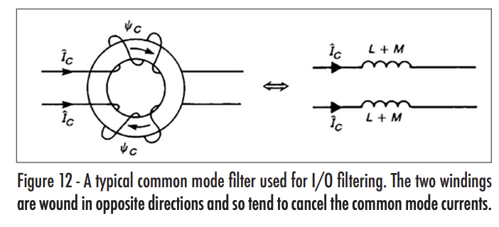
Filtering I won’t go into very much detail here, because Interference Technology has an excellent EMI Filter Guide free for the downloading (see Reference 8). Suffice to say, filters, as well as transient protection, are important at power and I/O connectors. Typically, these will be common mode topologies, as shown in Figure 12. Most signal-level common mode chokes may be obtained in surface mount packaging. Power chokes are much larger to handle the current and may be obtained as either surface mount or throughhole mount, depending on the current rating. Many Ethernet connectors have built-in common mode filtering.
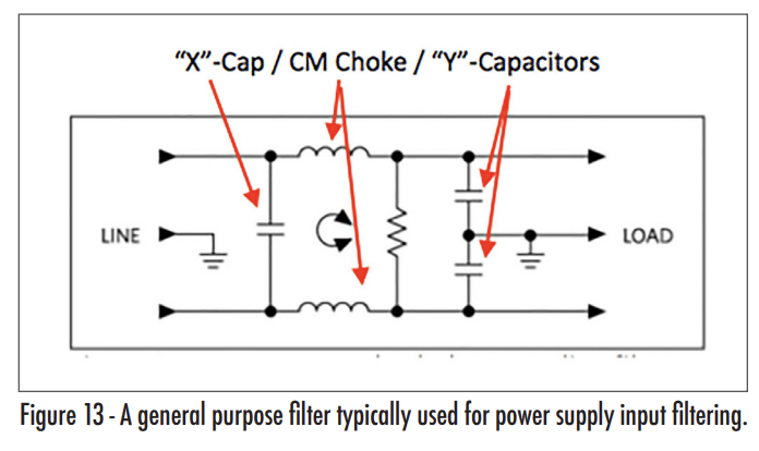
Power supply input filters are generally designed to suppress both differential and common mode currents. A typical topology is shown in Figure 13. The “X” capacitor is designed to filter differential mode, while the CM choke and “Y” capacitors are designed to filter common mode. The resistor shown is usually 100 kOhm and the purpose is merely to bleed off the line voltage stored on the capacitors to a safe level.
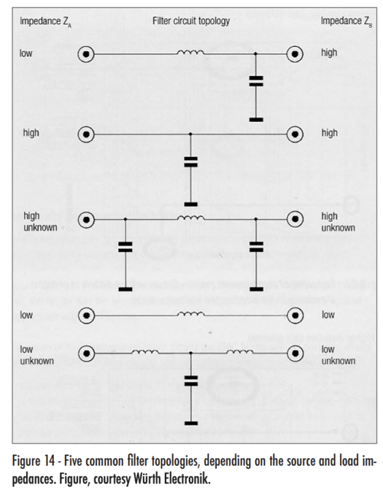
For general purpose filtering of signals, the handy chart of possible filter topologies may be found in Reference 9 and is reproduced here in Figure 14. The appropriate topology depends on the source and load impedances. If these impedances are not known, then either the “PI” or “T” topology may be used (#3 or #5 on the chart, respectively).
Ferrite or inductive components should not be used in series with the power pins of ICs, as this will only reduce the ability of the local decoupling capacitors to supply required energy during simultaneous switching of the IC output stages with the resulting higher power supply noise.
Ferrite Chokes – One common filter element usually added to I/O cables is the ferrite choke. Ferrite chokes come in either the clamp-on types or solid cores meant to be assembled along with the cable assembly. Often, these are used as a last resort to reduce cable emissions or susceptibility.
Most ferrite chokes have an associated impedance versus frequency characteristic, often peaking around 100 to 300 MHz. Some materials are designed to peak below 100 MHz for lower frequency applications. Maximum impedances can range from 25 to 1000 Ohms, depending on the ferrite material used and style of choke.
Sometimes, clipping a ferrite choke onto a cable has no effect. This is usually due to the fact the choke has the same, or lower, effective impedance than the cable itself.
The attenuation of a ferrite choke is easily calculated.
Attenuation = 20 * log((10 + 100 + 10) / (10 + 10)) = 15.5 dB
Refer to Reference 9 for much additional detail on ferrite chokes and general filter design.
Transient Protection
In order to protect internal circuitry from electrical transients, such as ESD, electrically fast transient (EFT), or power line surge, due to lightning, transient protective devices should be installed at all power and I/O ports. These devices sense the transient and “clamp” the transient pulse to a specified clamp voltage.
Transient protectors in signal lines must generally have a very low parallel capacitance (0.2 to 1 pF, typical) to the return plane, depending on the data rate in order to maintain signal integrity. These silicon-based devices may be purchased in very small surface mount packaging.
Power line surge protection usually requires much larger transient protection devices and they can come in a variety of types. Gas discharge or metal oxide varistors are the most common, but larger silicon-based devices are also available. More information on the design of surge protection may be found in Reference 4.
Summary Most EMC/EMI failures are due to poor shielding, penetration of cables through shields, poor cable shield termination, poor filtering, and above all, poor PC board layout and stack-up. Paying attention to these common design faults will pay off with a lower risk of compliance failures and result in lower project costs and schedule slippage.
References
1. Bogatin, Signal Integrity – Simplified, Prentice-Hall, 2009.
2. Morrison, Grounding and Shielding – Circuits and Interference, Wiley, 2016.
3. Morrison, Digital Circuit Boards – Mach 1 GHz, Wiley, 2012.
4. Wyatt, Gaps in Return Planes – Bad News for EMI (with video demo), https://interferencetechnology. com/gaps-return-planes-bad-news-emi/
5. Ott, Electromagnetic Compatibility Engineering, Wiley, 2009.
6. André and Wyatt, EMI Troubleshooting Cookbook for Product Designers, SciTech, 2014.
7. ITEM, 2016 EMI Shielding Guide, http://learn. interferencetechnology.com/2016-emi-shieldingguide/
8. ITEM, 2017 EMC Filters Guide, http://learn. interferencetechnology.com/2017-emc-filters-guide/
9. Würth Electronik, Trilogy of Magnetics, 2010.
