Timothy Puls
Semtech Corporation
Ethernet is ubiquitous. From base station backhaul, to wireless access points, to IP surveillance cameras – Ethernet is found everywhere. And, the devices enabling this Ethernet traffic – the miniature transceiver ICs driving the communications infrastructure – are more advanced than ever before. Before 2010, Ethernet physical-layer transceivers (PHYs) were based on 90-nanometer IC technology. Today, the market has strongly adopted higher performance 65-nanometer PHYs with a plan toward 45-nanometer and below. While the newer PHY platforms give system designers exciting performance advantages, there is a menacing side effect felt by the EMC community – reduced on-chip ESD protection levels.
The mantra of the IC world – smaller is better – means chip manufacturers confront new trade-offs. As IC technology leaps forward to achieve aggressive die size and performance targets, the protection clamps at the chip I/O are often compromised. This, of course, is not without impact to the system level robustness of the transceiver interface.
While chip manufacturers are squeezed by the physical constraints of implementing protection on the chip, the system designer is likewise squeezed with the challenge of engineering an end product that will prove robust against the many electrical transient threats encountered by the end product. And, the system-level transient immunity standards are not easing. Quite the contrary – more stringent requirements are emerging.
SYSTEM LEVEL TRANSIENT THREATS
In years past, protection circuitry was something of an afterthought in the design cycle. Today, few debate the necessity of external protection arrays, and increasingly designers appreciate the value of a well-conceived circuit protection plan on the front end of the design phase.
This is especially true on Ethernet ports. The racks of twisted-pair cable within the network infrastructure need a resilient defense against a variety of transient over-voltage threats – electrostatic discharge (ESD), cable discharge (CDE), electrical fast transients (EFT) and, of course, highly destructive lightning surges.
The goal of a good protection scheme has two parts. First, the protection must safeguard the PHY from the transient threats encountered. Secondly – and maybe more challenging – the protection circuit should be benign with respect to the signal transmission of the link. As the landscape has changed from Fast Ethernet to Gigabit Ethernet to 10Gigabit Ethernet, this is now a more challenging proposition.
A good defense must take into account the characteristics of the threats. At a most basic level, transient threats can be divided into two broad categories: fast rise-time threats and slow rise-time threats. The way in which these spikes couple into ports and onto PCB traces can be quite different, and the type of components needed to arrest them can be different.
ESD, CDE (Cable Discharge) and EFT (Electrical Fast Transients) are fast rise-time events; they have a rise-time on the order of 1 nanosecond (often less than 1 nanosecond). For the purposes of this discussion, we categorize these three events broadly as fast rise-time transients, but it is worth noting that these transients behave somewhat differently. The energy within a CDE strike or an EFT burst can prove more cumbersome to tame than an ESD event generated by human contact. The top row of Table 1 highlights some notable differences in these pulse characteristics.
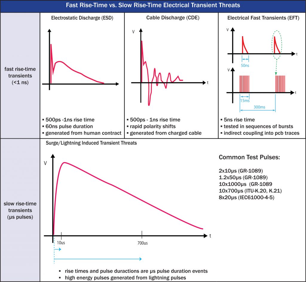
The second class of transient threat is the surge threat. Surge events are slow rise-time lightning induced pulses. These waveshapes are generally microsecond events. They have slow rise times compared to ESD, CDE and EFT, but present orders of magnitude higher power in the pulse shape. They can be defined as either a voltage waveform with a peak voltage or a current waveform with a peak pulse current. In segments of the telecom market, end equipment manufacturers may demand very high levels of immunity from lightning induced threats. The bottom row of table 1 shows some common test pulses used to show immunity to lightning induced surge.
TRANSIENT VOLTAGE SUPRESSION (TVS) ARRAYS
The challenge in protecting Ethernet ports is that the end equipment may be exposed to all these different transient types. Thus, it demands versatility out of a protection structure. Where yesterday’s system designers could choose from a variety of low-end circuit protection components, today’s systems require a bit more care and attention in selecting an optimized solution.
Due to their low voltage breakdown, fast response time, and low clamping voltages, Transient Voltage Suppression (TVS) diodes offer some unique advantage for safeguarding low-voltage Ethernet lines against a range of transient threats. Other components can be used, of course, but at some level a TVS device is likely required.

How TVS Diodes Work
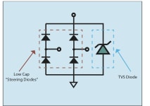
TVS diodes are overvoltage protection elements that connect as shunt devices across a data line (Figure 1). Under normal signaling conditions a TVS diode presents high impedance. The TVS device has a rated capacitance and a rated leakage current typically measured at 0V and the device working voltage respectively. These parameters should be chosen appropriately for the speed of the signal interface and also sufficiently minimized such that the TVS diode appears “transparent” to the circuit during normal operation.
When a transient spike hits the port the TVS diode acts like a “trap door” to ground for the transient current. The diode junction achieves breakdown and becomes a low impedance shunt path to sink dangerous current through the diode junction. An effective protection circuit diverts this transient current and clamps the transient voltage spike to a level below the failure threshold of the protected IC.
Especially for the fast rise-time events (ESD and cable discharge) the diode junction must breakdown at a low voltage threshold to engage the transient during the initial inductive spike, In the case of lightning the TVS junction must absorb the high surge currents. As such, the TVS junctions are larger for a lighting rated device.
For silicon TVS junctions, there is a trade-off between the current handling of the device and the capacitance. As a basic rule, the higher the value for the max peak pulse (Ipp) rating of a TVS part, the higher the capacitance of that device. And, conversely, a device with a low capacitance generally correlates to weaker surge absorption.
On Ethernet lines, the device must present a robust surge rating without introducing an excessive capacitance load that will disturb signal quality. TVS arrays can achieve such high-surge immunity and a low capacitance with a “rail clamp” diode architecture. By bridging a TVS diode with very low capacitance “steering diodes,” the effective capacitance of the TVS array can be minimized while also upholding the surge rating (Figure 2a).
Clamping Voltage
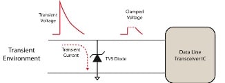
In evaluating how well a protection array is “protecting” the clamping voltage must be considered. The clamping voltage is the voltage resulting after the TVS device has clamped the incoming surge transient. (See Figure 2b) This “clamped voltage” will appear at the PHY input. Obviously, it should be minimized. The lower the transient voltage is clamped, the better the protection margin. It is here where the TVS selection makes all the difference.
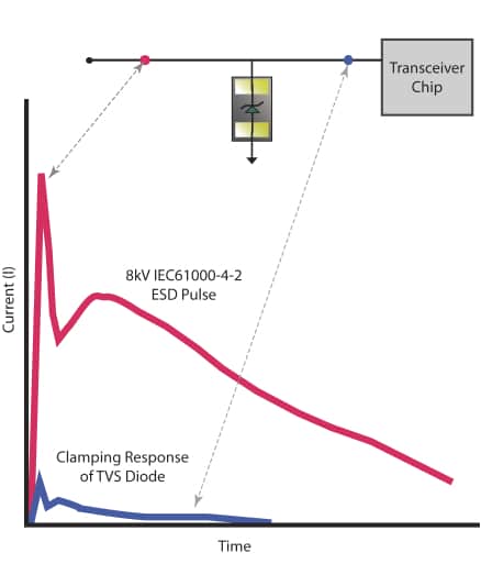
A device with a lower working voltage can help. This is the normal dc operating voltage of the TVS. Below the working voltage the TVS device is a high impedance element. Just above the working voltage the TVS begins to conduct current. For optimal protection, it is preferable to choose devices with a low working voltage. As an example, for Gigabit Ethernet ports where the differential signal swing may be just under 2V, a TVS with a working voltage of 2.5V will typically have some clamping advantages over a device with 6V. The lower working voltage allows the TVS to arrest the voltage spike at a lower voltage threshold and in theory respond faster.
Additionally, a TVS with “snap back” I-V characteristic can also bring some advantage. In this case, there is a slight negative resistance in the I-V curve. This yields steeper I-V curve, which, in turn, can help lower the clamping voltage at the peak pulse current (see Figure 3).
TVS clamping voltage for a lightning condition is often benchmarked using an 8×20µs current pulse. The following 8x20us clamping voltage curve illustrates the divergence of differing TVS devices in clamping voltage. As the silicon PHY scaling continues leading to more sensitive IC interfaces standard 5V zener arrays are hardly suited to protect high-end Ethernet systems. Instead, low working and low clamping voltage are needed.

CIRCUIT PROTECTION IMPLEMENTATION

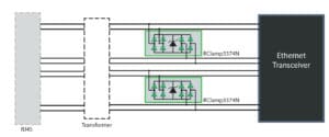
Finally, the question frequently arises as to where the protection devices should be implemented. Is it better to place the protection on the line side closer to the boundary of the port? Or is it better to place the protection on the PHY side behind the Ethernet magnetics? There are certainly good reasons for choosing either. Yet, for most immunity conditions, the advantages to protecting on the PHY of the Ethernet magnetics outweigh the advantages to protecting on the line side. One of the key reasons for PHY side protection is that for most surge events, the transformer provides some level of attenuation to the surge event. Thus the pulse is reduced somewhat on the PHY side of the interface – though it is still an extremely dangerous surge. Placing components on the PHY side allows the EMC immunity plan to leverage the transformer and whatever action it is providing against the surge.
CONCLUSION
The Ethernet ports in today’s networking landscape are more sensitive than any other previous time within the industry. Power efficient, highly miniaturized Ethernet PHYs increasingly need advanced transient voltage protection circuits to safeguard against a host of transient threats. With some forethought at the outset of the design phase, TVS diodes can be effectively implemented to safeguard Ethernet-based systems from the many transient voltage threats encountered at the system level.
Tim Puls is a product marketing manager for protection products at Semtech. Previously, he worked as a field sales engineer with National Semiconductor and in application engineering for Texas Instruments. He holds a bachelor’s in electrical engineering from Texas A&M University. He can be reached at tpuls@semtech.com.


