Wireless/RF is ubiquitous, so implement a pre-compliance regimen with off-the-shelf equipment.
Every electronic product has to go through full electromagnetic compatibility (EMC) testing to get the much-coveted stamp of approval from the various regulatory bodies. This has traditionally been a costly undertaking with multiple trips to a distant testing facility, with multiple reworks required to get final approval. In the age of the Internet of things (IoT), this is not the way to go about it. There is a better approach.
The IoT has changed everything, with wirelessly connected devices creating the opportunity to gather data to perform analytics in order to improve device usability for consumers. For industry, IoT-enabled analytics are improving process, safety, and production outcomes for manufacturing facilities, while opening the possibility of new business models. However, for electronic system and consumer product designers, it has created a number of headaches; some obvious, some more subtle and insidious.
To start with, there’s the ubiquitous demand for wireless connectivity, whether it be Wi-Fi, Bluetooth, Zigbee, cellular, or the various flavors of long-range, low-power options such as LoRaWAN, Sigfox, Narrowband-IoT (NB-IoT) or LTE Cat 1. It’s common to have multiple RF interfaces in the same device. This is great for users, but is a nightmare for designers, many of whom are not RF experts. They may have mastered the art of ensuring power supplies no longer interfere with digital circuits, but wireless connectivity adds a whole new dimension of difficulty. From the antenna placement and routing, to the design of high-frequency circuits from 900 MHz to 5 GHz, the difficulties have affected many product delivery schedules, and the problem is only going to get worse with 5G emerging with millimeter-wave operation at 28 GHz and up.
Brave designers will “roll their own” RF circuits, but these tend to be large design teams with high-volume expectations. It seems easy enough, get a good RF integrated circuit (IC) from a reputable vendor, put some shielding around it, place and route the antenna wire, and they’re off and running. Maybe. However, a few trends have altered the design landscape and have forced designers to rethink their approach.
The primary influences on designs are smaller form factors, higher integration and electronic component density per inch squared of printed circuit board (PCB) space, system complexity, higher clock speeds, multiple and distributed power rails with fast-switching transients, LCD emissions as displays get integrated into IoT devices, and faster data transfer rates between Central processing unit (CPU) and memory. These are the obvious and classic trends that create interesting challenges that designers actually enjoy solving, though time-to-market pressures and shrinking budgets can be a kill-joy for some, or an added challenge for others.
However, as mentioned, there are two more subtle trends, and these are the ones that are actually causing the most headaches, and the most opportunity for differentiation through innovative approaches to expediting the route to ensuring system EMC.
These trends, which are a direct result of the IoT, are the need to combine power supplies, high-performance digital circuits, and RF interfaces in compact form factors for products that are falling rapidly in price. So much so, that the complexity-to-price ratio is becoming untenable for high-quality, low-cost smart-home-based systems that are the sweet-spot for IoT devices. Even mobile phone and tablet manufacturers, which have typically been able to charge a premium for higher margins, are getting squeezed as complexity increases and form factors shrink.
To address EMC and its associated electromagnetic interference (EMI) issues, it used to be sufficient to place shielding around key components, such as the RF circuits, to reduce their susceptibility to interference from high-speed digital clock and signal switching harmonics, and to prevent them from being an interferer. However, as density and complexity has increased, it’s now not uncommon to shield literally everything, as in the case of the Samsung Tab S4, Figure 1.
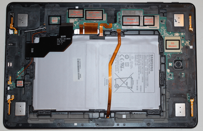
Figure 1: It used to be sufficient to shield a couple of key circuits, but the designers of the Samsung Tab S4 tablet shielded literally every circuit to ensure maximum EMC. The four rectangular silver elements on the corners are speakers, not circuits. (Image source: Rohde & Schwarz)
The Tab S4 is an extreme example of cutting-edge consumer-level design in terms of density, performance, and complexity, with a price to match ($649). However, most designs in the IoT space, from white goods and audio streaming systems with built-in voice assistants, to wearables, cost much less, forcing designers to find ways to lower development and test costs.
Accelerating EMC Testing – While Lowering Cost
It’s possible to accelerate the design and test cycle when using power-supply and RF modules. These come pre-certified and do save time and resources. However, many designers falsely assume that buying a module means they’re home free with respect to national and international compatibility and compliance regulations. Nothing could be further from the truth.
It’s true that the RF module may remain fully Bluetooth certified and interoperable, but once the power supply, RF module, antenna, and digital circuits are laid out and connected all regulatory certification bets are off. The full system now needs to be certified to CE, FCC, or CISPR requirements, due to the many and varied interactions between the subsystems. These include load transients, spurious power-supply emissions, various internal and ambient EMI sources, and RF harmonics.
The task for designers is to understand EMC and the effects and sources of EMI, and then performance pre-compliance testing on the system to identify and mitigate any issues – before sending it out to an external lab for certification. Along with the expense of time, the compliance tests themselves can cost up to $10,000 and up to 90 percent of devices fail the first time around, leading to rework and retesting, sometimes multiple times. The costs add up quickly, especially if the fix requires a full or partial redesign. It’s critical to initiate preventative measures, such as design-cycle checkpoints, to help avoid costly project delays, Figure 2.
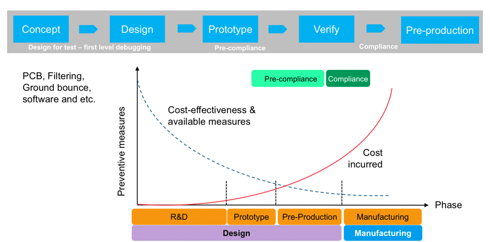
Figure 2: Implementing a regimen of pre-compliance checkpoint tests can greatly increase the chance of completing an IoT design on time and within budget. (Image source: Rohde & Schwarz)
Another important reason to perform pre-compliance testing is to avoid over-design of the device. Often, designers run the risk of adding additional shielding or other precautions, which adds weight, time, power consumption, and direct costs. The goal is to pass the test for full compliance without going overboard.
In order to minimize the chance of multiple rounds of compliance certification and rework, it helps to have some up-front education on EMC and EMI. Combined with off-the-shelf test equipment and some “tricks of the trade,” it’s possible to quickly identify and mitigate EMC issues before submitting a system for formal certification.
Defining EMC and Identifying Sources of EMI
EMC and EMI are often confused, but simply put, EMC is concerned with ensuring various pieces of electrical and electronic equipment can operate in the same electromagnetic environment. It requires the equipment to have minimal unwanted electromagnetic emissions and to also minimize its susceptibility to ambient electromagnetic energy, typically from nearby equipment or long-range radio transmitters.
EMI is the actual unwanted electromagnetic energy that designers need to suppress within their own designs, as well as protect their design from outside sources. These sources can be static electricity, other radios, sporadic emissions from motors or power supplies, mains hum, microwave ovens and the system’s internal digital switching harmonics and sub-harmonics, and even audio signals. Their interference potential depends upon the operating frequency of the equipment under test (EUT) and they can manifest as continuous wave or pulsed EMI signals.
In EMC parlance, the system causing the interference is the source, and the system being affected is the victim. Between them are the four EMI coupling mechanisms: radiated, inductive, capacitive, and conductive, or any combination of the four, Figure 3. EMI can be viewed fractally in the sense that it applies between small or large systems that are near or far apart, as well as between subsystems, components, traces, and antenna within a system. Not that antennas are particularly interesting, as they not only transmit and receive intentional emissions, but also serve as perfect couplers of EMI into and out of a system.
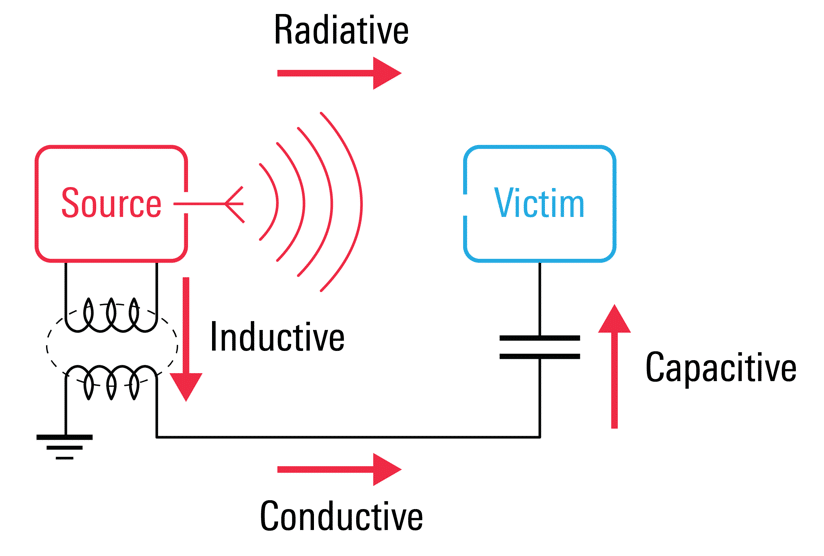
Figure 3: The four EMI coupling mechanisms are radiative, inductive, capacitive and conductive. (Image source: ipfs.io)
The EMI and EMC principles are similar for nearby and within systems. For the sake of simplicity, this article will focus on a single system and how to design for EMC, perform pre-compliance testing, and debug using an off-the-shelf, mid-range oscilloscope.
Designing for EMC
Let’s consider the following basic principles to demonstrate that EMC hasn’t changed since EE 101:
- Be careful on trace routing
- Be aware that higher speeds mean more EMI issues
- PCB stacking makes EMI worse
- Avoid sharp corners in traces (reasonable design tools can match the maximum trace angle to the operating frequency)
- Have larger ground planes
- Use shielded cables and housings
- Avoid discontinuities and resonances in the transmission path
Unfortunately, EMI cannot be eliminated entirely. Thus the designer’s job is to manage and mitigate it, applying fundamental principles in combination with experiential know-how.
Pre-Compliance Test and Debug
Once the design is in the prototype stage and pre-compliance checkpoints have been established, the next task is to either isolate the EUT completely from ambient EMI, or to characterize the environment and account for detected interferers during the test cycle. Again, interferers also cannot be eliminated, but the probability of interference can be determined and mitigated.
To scan a wide range of frequencies for interferers, a full EMI receiver with an array of filters and wide dynamic range is a good option, but can be expensive. Alternatively, a spectrum analyzer can come close to an EMI receiver’s capabilities without breaking the bank. Start by getting a baseline and account for any present signals. Spectrum analyzers, such as the R&S®FPC1500, have optional PC EMI software (Elektra) that can set the compliance limits, or the user can do it manually, Figure 4.
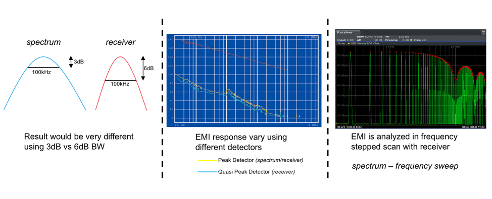
Figure 4: When in receive mode, spectrum analyzers can imitate higher cost EMI receivers, but make sure it has at least a quasi-peak (QP) detector with a directional antenna. (Image source: Rohde & Schwarz)
The spectrum analyzer itself will need at least a quasi-peak (QP) detector with a directional antenna as part of the minimum viable feature sets to approximate a full EMI-compliant receiver. Look for an analyzer with a frequency range from 5 kHz to 5 GHz to detect sub-GHz signals and 5-GHz Wi-Fi network interferers. Also, a built-in vector network analyzer (VNA) is useful as it can be used to match the antenna impedance to the RF module if there isn’t an RF antenna built in. Some spectrum analyzers also have an integrated signal generator that can be used to generate an additional signal in the presence of the intended transmitter signal. This “interferer” tests to make sure there is sufficient blocking at the receiver to allow the intended signal to get through.
To start pre-compliance testing, do a limit-line test, or max hold sweep, with a max hold detector, as that’s a fast and easy test. Then, use the QP detector to do spot checks on any potential problem areas. Use electric field (E-field) and magnetic field (H-field) near-field probes, Figure 5. The magnetic field probe has a loop through which the magnetic field passes perpendicularly, inducing a detectable voltage.
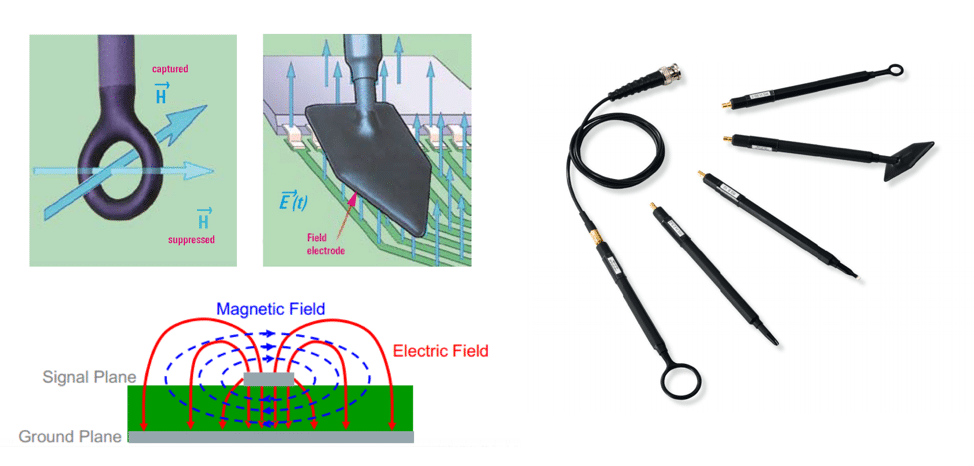
Figure 5: The larger the size of the E-field and H-field probes, the greater their sensitivity, at the cost of precision. It helps to zero in on the EMI source by reducing the size of the probe. (Image source: Rohde & Schwarz)
When using the probes, it’s important to keep in mind that the output of the probe very much depends upon the orientation of the probe relative to the emitters. Also, there is a trade-off to be made: the larger the probe, the greater the sensitivity, but the precision decreases. So, as the source of EMI gets more clearly defined, reduce the size of the probe to zero in on the source and verify that the readings are below the maximum power levels allowed.
This requires having a solid knowledge of the design to know where these might be. Many EMI sources can be anticipated by factoring in the clock frequencies, the power supply’s switching frequency, and the expected harmonics.
Knowing the layout is critical as it helps to know when a clock line might be too close to an RF module. This becomes something to watch for as it might be what’s coupling in and causing another spur that’s in a different part of the spectrum.
However, no matter how good a designer’s knowledge of the physical layout and the circuit’s design parameters, nothing beats running the system software and time-correlating the EMI to the running code.
Time-Correlated Test and Debug with Oscilloscopes
Given the budget and resource constraints of many IoT developers, a spectrum analyzer may be out of reach. However, every bench has an oscilloscope, and the right digital oscilloscope can also perform EMI test. This was not always the case, as the fast Fourier transform (FFT) processing capability wasn’t available. That has changed, with some digital oscilloscopes now implementing FFT digital down-conversion and overlapping FFTs in hardware.
Look for a digital oscilloscope with these key characteristics: enough capture memory (can hold greater than 500 Ksamples), 50-Ω coupling impedance to ensure sufficient bandwidth and a sample rate >2x the maximum frequency, start with 2.5 Gsamples/s for 0 to 1 GHz. If testing systems with 2.45-GHz or 5-GHz radios, the sample rate will need to be upgraded accordingly. Also look for low noise and good vertical sensitivity capable of being set to 500 µV/div to 5 mV/div for high sensitivity over the full bandwidth.
As the probe will be moving around the board or system, it’s important that the scope’s response time be fast so there’s no delay when trying to correlate EMI back to the time domain. Some scopes do include FFTs in software, so be careful to ensure the time and frequency domain are seen in real time. As the source of the EMI becomes clearer, the time-domain view should allow the EMI source to be correlated to changes such as bus level switching, Figure 6.
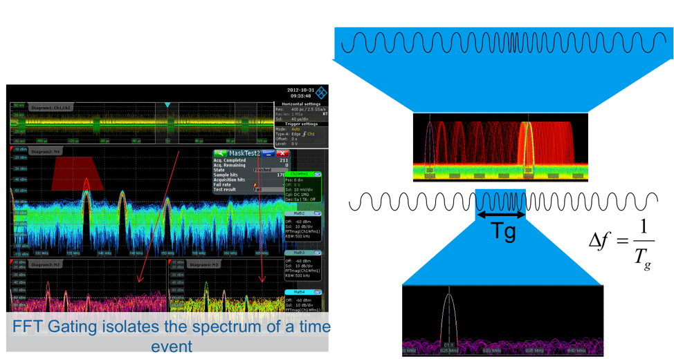
Figure 6: Multi-domain digital oscilloscopes with fast FFT capability and a gating feature help debug by allowing users to time-correlate EMI events and find their origin. (Image source: Rohde & Schwarz)
Other features to look for on a scope include a color table and screen persistence to easily detect and distinguish continuous wave signals, burst signals, and signal zoom. These are typical features of the R&S®RTE1000 or R&S®RTO2000 oscilloscopes, Figure 7.
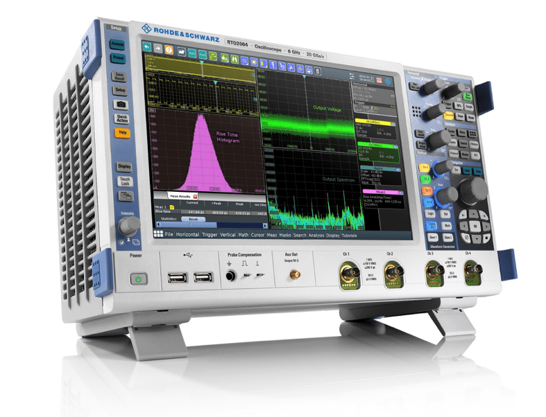
Figure 7: The R&S®RTO2000’s 10.1-inch capacitive touchscreen allows users to quickly navigate pop-up menus and adjust scaling by zooming in or moving a waveform. (Image source: Rohde & Schwarz)
Conclusion
In the age of IoT, with ubiquitous wireless connectivity, meeting EMC requirements for any standard is becoming more difficult and time consuming. The problem is exacerbated by the falling cost of IoT devices, which puts pressure on designers to get it right the first time to avoid extra certification costs and rework. That said, implementing a strict pre-compliance test regimen and checkpoints combined with typical benchtop equipment, such as digital oscilloscopes, can help limit formal and expensive EMC certification testing to one round.


