Patrick Carrier – Mentor Graphics, a Siemens Business
Antennas come in all shapes in sizes. In addition to wireless communications, they are becoming ubiquitous in the automotive space as well. Similarly, very high speed digital circuits are pervading these realms. It is the unintentional creation of antennas in these high speed digital circuits that cause Electromagnetic Interference (EMI) issues. One of the main goals in designing a high-speed circuit is to make it a very poor antenna; in other words, make sure all currents are traveling in a closed loop. The ramifications of failing to doing so include failing emissions requirements, increased susceptibility to outside noise sources, and unreliable circuit operation.
Designing a digital circuit with closed current loops seems simple enough, but where are the loops? The answer to that depends on a few factors, including whether the circuit is doing a 0-to-1 or 1-to-0 transition, how the transmission lines are referenced, and where the decoupling capacitors are located. In Figure 1 below, we examine the current loops for a fairly common case. An I/O buffer is connected to a transmission line that is referencing both power and ground planes. In a 0-to-1 transition, current is going to come from the power pin to the power plane connected to the buffer, down through the pull-up transistor, out onto the trace, where it will couple onto both planes. It will then flow on the ground plane back to the ground pin, and on the power plane through the decoupling capacitors to ground.

Figure 1. Current loops in a high speed digital circuit
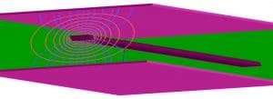
We often refer to the currents in the planes as return current. They are the result of energy coupled from the trace to the planes through electromagnetic waves. The potential of the planes does not matter. Whether they are a ground plane or a voltage plane, at any given instant, the trace will be coupling energy into its reference planes. It will actually couple energy onto whatever are the nearest pieces of metal, but in most well-designed PCBs, those are usually planes. If those planes happen to be the power and ground planes used by I/O buffers driving that trace, that is the best case, as it best facilitates a complete loop for the return current. Figure 2 depicts the field coupling between a trace and its reference planes.

Figure 2. Field coupling of a trace and its reference planes
That coupling determines the electrical properties of the trace, like the impedance of the trace. It can be described as inductance and capacitance per unit length. As the signal travels down the line, it is effectively charging up each of those LC circuits, and then moving on to the next one, charging that one up, and so on. Any break in that circuit will cause radiation to occur. Obviously, you wouldn’t expect the circuit to work if you cut the trace (other than it acting like an antenna). A cut in the reference part of that loop can have the same effect. It is important to remember that a transmission line is a combination of a trace and its reference plane, and keeping them both in good shape will eliminate most EMI problems. The best way to avoid creating unintentional antennas is to keep the return current adjacent to the trace and on the reference plane(s).
There are a number of ways to work around traces crossing reference plane splits. Of course, it would be best to route all signals referenced to a solid ground plane, but board thickness and cost concerns often do not allow this. However, through careful stackup planning, you can route slower signals against any power planes that will be split up among multiple different voltages. Even if this is done, it usually involves a dual stripline trace structure, which utilizes two reference planes for two trace layers. A trace will be more closely coupled to its nearer reference plane, allowing it to cross a split in the further reference plane. The return current distribution scales linearly with the distance of the trace to its reference plane. So, if a trace is 4 times closer to its nearer reference plane than the further plane, that plane will have 4 times the return current.
A common method used to minimize radiation from traces crossing plane splits is to stitch the planes together in the vicinity of the trace crossing using decoupling capacitors. This can be somewhat effective, however, it is important to note that a mounted capacitor does not act as a low impedance across a wide frequency band, so it will not eliminate the radiation issue.
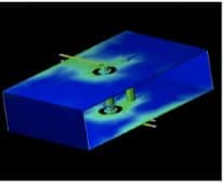
Less extreme but equally problematic are situations where the return current path is not completely broken but compromised. A common example of this is the case of a signal transitioning between layers using a via. As the signal transitions, there needs to be some path for the trace return current to connect between reference planes. If the trace is transitioning between layers where the reference planes are the same potential, such as all ground referencing, such a path can be created using a stitching via. If, however, the referencing changes from all ground to all power, the planes must be stitched together using a bypass capacitor or, better yet, a network of bypass capacitors. Such a network of capacitors is already present in the design as part of the PDN. Decoupling capacitors are connected between power and ground, usually in the vicinity of the IC, so if a layer transition has to be made, it is best to make that transition near an IC where these capacitors are. Another way of looking at that is to “pick a layer and stick with it”; in other words, make the layer transition at the IC and continue the route on that layer until it is at another IC.

Figure 3. Current distribution for a signal via with a nearby transition via
Another example of a compromised return path is a signal being routed close to the edge of a reference plane. Not only does this change the impedance of the trace, but it also will cause some radiation and make the signal more susceptible to noise. Issues like this can difficult to find in a layout, as they often result from regular voids in the planes from via antipads and mounting hole clearances.
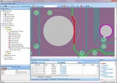
Finding such issues often requires a tedious manual design review of the layout. But these issues can be found quickly using an automated design rule checking tool such as HyperLynx DRC. An example is shown in Figure 4. Such design rule checks can be automated and customized to go beyond just a simple check of a trace near a hole, to include an understanding of return current distribution near a plane edge.

Figure 4. Trace near reference plane edge identified and highlighted in HyperLynx DRC
Other issues can be found through automated inspection as well, such as the low-inductance connection of decoupling capacitors in the vicinity of the power and ground pins of an IC. Decoupling capacitors are needed at ICs to complete the return current loop even if there are no splits in the plane. This can be seen in Figure 1, where the decoupling capacitors are depicted as a single capacitor. If the trace is located symmetrically between the two planes, half of the return current will flow into the power plane and need to make its way to the ground pin. This is where decoupling capacitors placed at the IC allow that current to flow from the power plane to the ground pin. That makes decoupling capacitors as essential to controlling EMI as they are for maintaining power integrity.
EMI issues are related to both power integrity and signal integrity. An inadequately designed power distribution network (PDN) will lead to radiated emissions, usually corresponding to the high-impedance points of the PDN profile. For signals, if a signal is radiating energy, that also means that energy is not making it to the receiver, causing a signal integrity issue. This is usually manifested as edge degradation. Signal and power integrity issues are usually solved through analysis and subsequent design changes. Solving EMI issues involves ensuring complete current loops, which can be accomplished through careful inspection of the board. Reviewing all possible EMI issues on a board can be complicated and time-consuming, and made more practical by the use of automated design rule checks. A combination of analysis and careful design review will keep you from creating unwanted antennas on the board, and leave your high speed interfaces running reliably and working well with the antennas that are supposed to be there.
