In this case study we’re going look at some recent radiated emissions fault finding we performed for a customer. This highlights how one might go about the fault finding process, some of the considerations you might have when coming up with a solution, and how poor PCB layout can give you an emissions headache.
Background
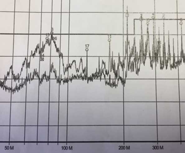
A new customer discovered a radiated emissions problem involving a product at an advanced stage in the production cycle. They had results (a low quality photo of scan result, Figure 1) from another test lab that showed a failure at two frequencies (with marginal results at others) and they needed some assistance in improving the EMC performance. The first thoughts when reviewing the failing results was that of power supply noise causing the broad hump around 80 MHz and then harmonics of a digital clock signal causing spikes from 130 MHz upwards.
Before any testing starts, it is important to understand the product in terms of cost sensitivity, product volume and design lifecycle as this will ultimately guide the work and the measures employed to improve emissions. There’s no point adding a $/€/£5 clip on ferrite core to a product that is high volume / low cost as this would affect the Bill of Materials (BOM) cost too much. Similarly, for a low volume high margin/value product there’s no point in redesigning the PCB to add a single common mode choke filter when the BOM cost could accept the more costly ferrite core which can be easily fitted in production with a single snap.
With this equipment falling into this latter category and being ready for production there was a desire to try and find effective modifications that could be easily applied without scrapping or significant rework of existing inventory and without incurring too many delays.
Experiments
The engineer from the customer was very enthusiastic and keen to learn more about EMC testing and the problem resolution process. It’s always a pleasure to work with people who are both interested and interesting and it was a most enjoyable time working with him. He had brought two units: one “vanilla” unmodified unit and one with a significantly modified wiring loom for experimentation. Needless to say, he was quite keen to know if the modifications he’d made with the wiring loom would improve the emissions.
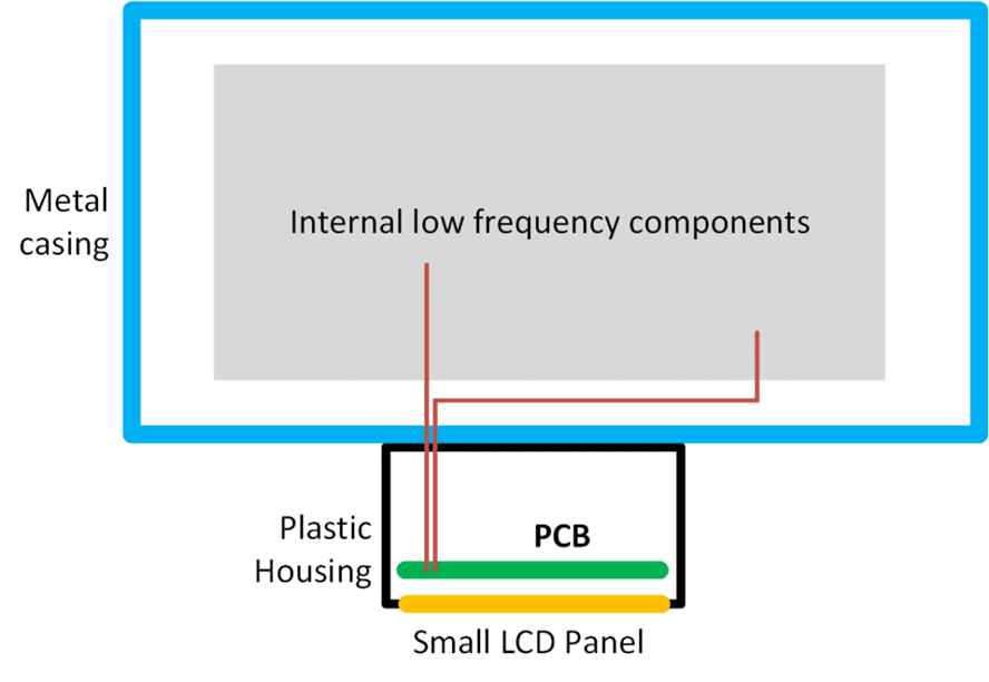
The product consisted of a two-part metal enclosure enclosing some low frequency control components with a plastic housing on the front of the unit housing a LCD panel, buttons and a control PCB.
The improved and shortened cable routing sample that the customer brought improved the emissions slightly but not to the point of passing the EN 61326-1 Class B limits. We spent a while disconnecting cables from the control PCB that sent us down a couple of false avenues; disconnecting the power lead giving the best results (I wonder why…). Similarly, removing the lid from the metal case, disconnecting internal components and removing all external cabling had very little effect. All of which pointed towards emissions directly from the PCB being the main problem.
Being systematic during such an analysis is very important, trying as best you can to change only one thing at once and always questioning your assumptions.
PC Board Noise Analysis
Near field probing using a 15mm diameter loop probe showed a little bit of pickup around the PCB. However, switching to a 1cm2 capacitive plate probe around the PCBs, power supply and cable assemblies showed that the noisiest area by far was the CPU / SDRAM interface with widespread harmonics from 84 MHz (the clock) up into the 1-2 GHz region. Using a pre-amplifier for this probing is a good way to get a lower noise floor – either the one built in to the spectrum analyser or a cheap external one will result in another 10dB of measurement range.
Probing the connector pins with a spectrum analyser, preamplifier and high bandwidth passive probe showed minimal energy at the frequencies of interest on the cables leaving the control PCB. The conclusion was that the problem was caused by direct radiation from the control PCB itself.
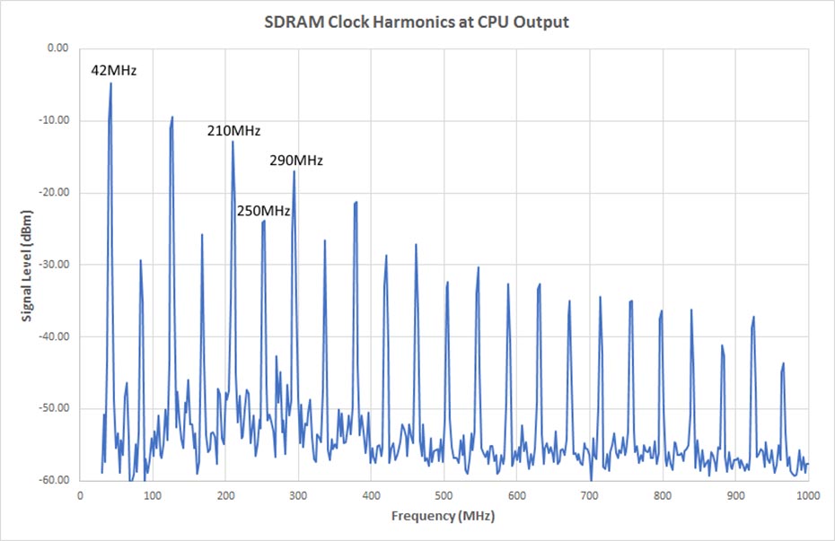
Measuring the SDRAM clock (Figure 3) with the spectrum analyser identified where the three most problematic peaks were coming from; all harmonics derived from the 42 MHz clock. The data and address lines in the interface will also have emissions based on these frequencies albeit the emissions are “smeared” over the spectrum due to the lower frequency and varying duty cycles of these signals. That is a topic for another article.
Well, since we know where it’s coming from what can we do about it without changing too much?
PC Board / Schematic Analysis
On visual inspection the PCB looked OK, perhaps lacking a few ground stitching vias, but not terribly laid out. It was only when the Gerber files were viewed in detail that several problems became obvious.
Whilst the PCB used 4 layers (good) it appeared to be under-utilised with no coherent solid planes or defined co-planar reference traces of any kind on any of the layers. In doing so the return path for the high frequency current was undefined resulting in the HF return currents finding their own uncontrolled route to minimise the loop area to the outbound trace, using stray capacitances to achieve this goal.
Take for example the SDRAM clock trace highlighted in yellow in the Figure 4.
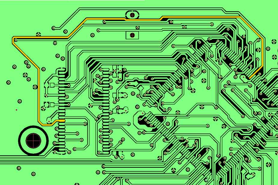
Bearing in mind that there isn’t a conventional ground or reference plane on the adjacent layer, where does the return current flow? Neither of the coplanar traces accompany the clock all the way back to the driver at the CPU end (on left). Just considering this very important trace the return path is compromised. You can also see the same thing for several other traces in this CPU <-> SDRAM interface.
So, whilst the PCB probably passed the Design Rule Check after what looked like an auto-route operation, the DRC doesn’t care about or understand EMC and signal integrity.
Fix
Re-lay out the PCB with coherent HF return planes and everyone is happy.
Meanwhile, back in the real world where the manufacturer has stock of the built up PCB and has invested a lot of time and money into the product development this isn’t realistic for getting the product out of the door.
The fix ended up being threefold:
- Turning on Spread Spectrum Clocking of the SDRAM interface. Changing the PLL configuration within the CPU to a 1% downspread of the clock reduces the energy at one specific frequency. This isn’t always available and shouldn’t be relied upon as a “get out of jail free” card but it certainly helps.
- Changing the SDRAM clock divider from 2 to 3 reduced the output clock frequency to bring some of the higher energy harmonics below the 230 MHz knee in the Class B limits giving increased margin in the key area of emissions.
- Scraping away top surface copper around mounting holes and addition of copper tape to display area.
(Side note: see this interesting article on the history of Spread Spectrum Clocking)
Modifications 1 and 2 are relatively easy to implement within the product firmware and help reduce the energy causing the emissions at source, the most effective way to solve an EMC problem. As for the last one? I hate to break out the copper tape. It’s a useful diagnostic tool but I always feel that it is a weapon of last resort when dealing with EMC problems. Despite the negative connotations (in my head) it is a good product to use in this situation being available off the shelf from a variety of manufacturers.
In this product the LCD panel had a metallic (possibly galvanised steel by the crystalline appearance) back plate with a conductive finish that just about covered the noisy traces on the PCB. The idea behind the copper tape was to provide a low(er) impedance path from PCB trace – radiated field – LCD panel rear – PCB “ground”.
Taking a cross section through the unmodified front panel (Figure 5) one would expect to see RF currents flowing through the stray capacitance between PCB and display as the HF current takes the lowest impedance (note not resistance) path back to the source that created them. The current flow through these capacitances creates the radiated fields measured by the antenna and receiver in the radiated emissions test setup. Reduce or control these currents and you can reduce the overall energy being delivered to the measurement system and improve your test result! This is the concept in placing an “image plane” near potentially radiating circuit traces, causing cancellation of the radiating fields.
(Side note: see this interesting article on the development and theory of the image plane concept, originally presented by Robert German, Henry Ott, and Clayton Paul in 1990 during the IEEE International Symposium on EMC).
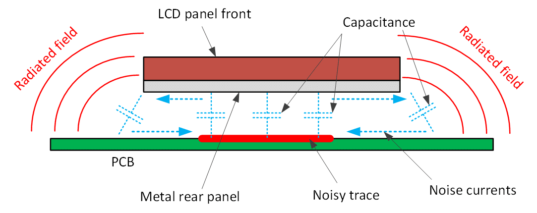
This is, of course, happening in three dimensions, which makes the visualization a little bit trickier to imagine.
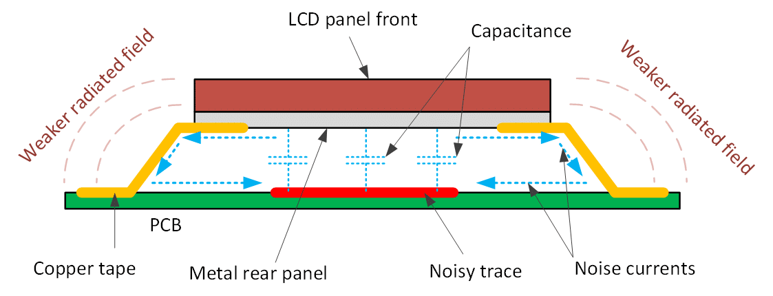
Now let’s take a look at the eventual modification. With the addition of the copper tape to connect the metallised LCD rear panel to the PCB (Figure 6) we are reducing and controlling the return path impedance. Whilst we aren’t reducing the levels of noise current we can at least give them a more readily defined path. Whilst this does not eliminate the radiated field entirely, it does reduce it significantly.
So how was this achieved in practice? Figure 7 shows the crude implementation during development. The conductive adhesive copper tape extends from the mounting bosses in the front panel plastic moulding (onto which the PCB mounts) and onto the metallised panel with sufficient area to form a good RF contact. Note that the capacitance of the two surfaces (tape and panel) in close proximity can be just as significant to the impedance as the actual resistance through the adhesive. Also, the top left piece of tape passes under the LCD control flexi PCB through a gap which is a bit of a fiddle to place but all part of the effective solution.
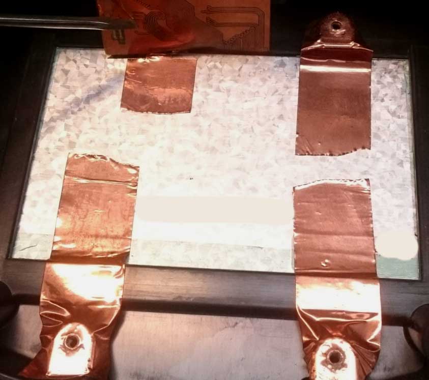
Figure 7: A crude but effective copper tape modification
This modification also necessitated scraping away the solder resist on the PCB around the PCB mounting holes and tinning the pads to provide a reliable electrical contact back to the PCB. This is easily achieved with a small hand held grinding tool like a Dremel running at low speed.
Outcome
This radiated emissions peak scan result shows the original unit as received from the customer (green) and the final modified unit at the end of testing (blue). The combination of the three modifications discussed above has ultimately reduced the emissions in the 180MHz to 350MHz band by up to 15dB with a 3dB margin in the 600 MHz to 900 MHz band. Improvements in this area would require a more complete shielding solution or preferably a re-layout of the PCB as mentioned above. Thanks to the addition of the Spread Spectrum Clocking, the Quasi Peak measurements were approximately 5dB lower than the peak readings below giving a better margin to the limit.
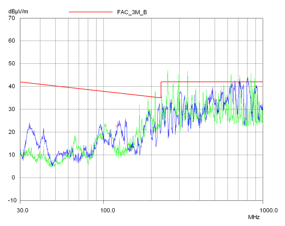
The customer wanted to close the loop by taking the product back to the accredited laboratory where they had conducted their original set of tests. A week or so later a call came through from them to say that it had passed with similar margins to that measured in our anechoic chamber.
As part of the follow up we delivered a full design review report and layout recommendations to the customer to aid their future development of the product line. Ultimately, we ended up with a happy customer with a compliant product and are now excited to be collaborating with them on a new design.
“This final report is a fascinating read and proves the value to be had by considering EMC at the very early stages of product design (not just PCB layout).
Many thanks for the support. We’ll certainly be in touch again.”
Conclusion
There are several useful lessons that one could take from this case study like “consider EMC at the start of the project” or “don’t operate your memory interface faster than you really need to”.
But the one thing you should take from this is get your PCB layout right.
There’s so much to discuss about this that it certainly lies outside the scope of this article. Books have been written about it. Big books. Most of the EMC problems you will face will be dictated, or at least heavily influenced, by the layout of the circuit board. This is where the noise is being generated after all!
If you have poor return paths for HF signals you will likely have radiated emissions issues to deal with. Fill your inner planes as much as possible with a good quality RF return path like a circuit ground and connect to it often. Avoid the use of the auto-router if possible or at least route the critical nets by hand. Think about loop areas, decoupling and transmission lines. Invest in training. Consider a 3rd party design review.
The consequences of a poor PCB layout? Hopefully you’ve just read about them.


