INTRODUCTION
Those graduating from university are often not trained in EMC.
When they are, they are most likely trained very well in the theoretical aspects of EMC or at least some physics. However, they often lack the ability to apply these theories to gain a hands-on understanding of EMC principles.
I have seen both junior and senior engineers struggling with aspects of EMC.
In my opinion, the problem is not with the engineers who are intrinsically very motivated but rather with the ‘electron-based’ theory taught at college and university.
Adopting wave-propagation-based thinking is often fairly difficult without years of experience and good guidance. For this very reason, the author developed an EMC Demonstration System in 2005 at the University of KU Leuven.
This system was inspired by Keith Armstrong’s original EMC Demonstration, built in 1990, and is now a full EMC Demonstration System.
VERY LIMITED EMC TRAINING AIDS AVAILABLE
It could be debated that there is a lack of EMC training tools available, with the exception of some very nice PCB design demonstrations. This is because integrating different demonstrations within ‘one unit’ or system is a huge and time-consuming challenge.
Remember physics in college? All ‘experiments’ were often isolated (non-realistic) situations, worlds apart from real-life applications.
In addition, it is fairly difficult for the untrained eye to ‘read’ and deduce the correct information from ‘dense emissions plots’ or see ‘any difference at all’ when the difference is very subtle.
Compare it with an X-ray image — we all can instantly spot a clearly broken bone, whereas a trained specialist needs to interpret more subtle details not immediately visible to the untrained eye.
THE EMC DEMONSTRATIONS
This being said, the EMC Demonstration Box evolved into a full EMC Demonstration System [1], [2], with two goals in mind:
- To teach and study EMC
- To clearly visualize some fundamental aspects of EMC
The EMC Demonstration System (EMD1), is an ideal tool to teach, study and clearly visualize:
- Shielding Effectiveness
- Impact of apertures (slots and holes)
- Impact of seams of the lid
- Conducted and Radiated Emissions levels
- Due to different PCB designs
- Impact of EMC filters and the importance of bonding
- Influence of shielded versus unshielded cables
- Influence of matched versus unmatched loads
- The relationship between conducted and radiated emissions
Enjoying this article?
Subscribe to Interference Technology for expert coverage of EMI, EMC, and signal integrity challenges—plus immediate access to new digital magazine issues.
Subscribe here →
REAL-LIFE DEMONSTRATIONS
Since then, the EMC Demonstration System has been used in many different settings:
- As a training tool for both bachelor’s and master’s students
- As a training tool within companies
- As a demonstration tool to the management of companies
- As a demonstration tool by EMC test labs, as a visual and practical aid to explain certain fundamental principles or needed design changes
- During EMC consultancy to quickly and easily explain principles
While training for a large international company and providing consultancy services, I encountered a recurring issue between the mechanical and electronic design teams related to enclosure design.
There were continuous back-and-forth discussions, and I was informed that this had been going on for years. Both teams struggled to fully understand each other’s requirements.
To address this, I decided to demonstrate differences in shielding effectiveness and emissions levels using the EMC Demonstration System, with both the mechanical and electronic design engineers present.
Almost immediately, the mechanical design team exclaimed, “Ah, this is exactly why the other team has those requirements!”
They had heard it many times before, but now they could literally and instantly see the impact of enclosure design and bonding options on the overall EMC of a product.
This demonstration effectively ended their ongoing discussions, and from that point on they became a much more efficient and cohesive design team.
COST AND ELECTROMAGNETIC ENVIRONMENT CONSIDERATIONS
Another challenge is the cost.
The EMD1 is a very affordable tool for both universities and companies. They gain additional insights which enable them to apply proper design techniques for good EMC as early as the prototyping phase, thereby saving huge amounts of money later during the development process — all while reducing debugging costs and overall test costs.
As a result, they decrease their time-to-market considerably.
I have seen companies saving tens of thousands of euros, dollars, and pounds by being trained with this aid in advance.
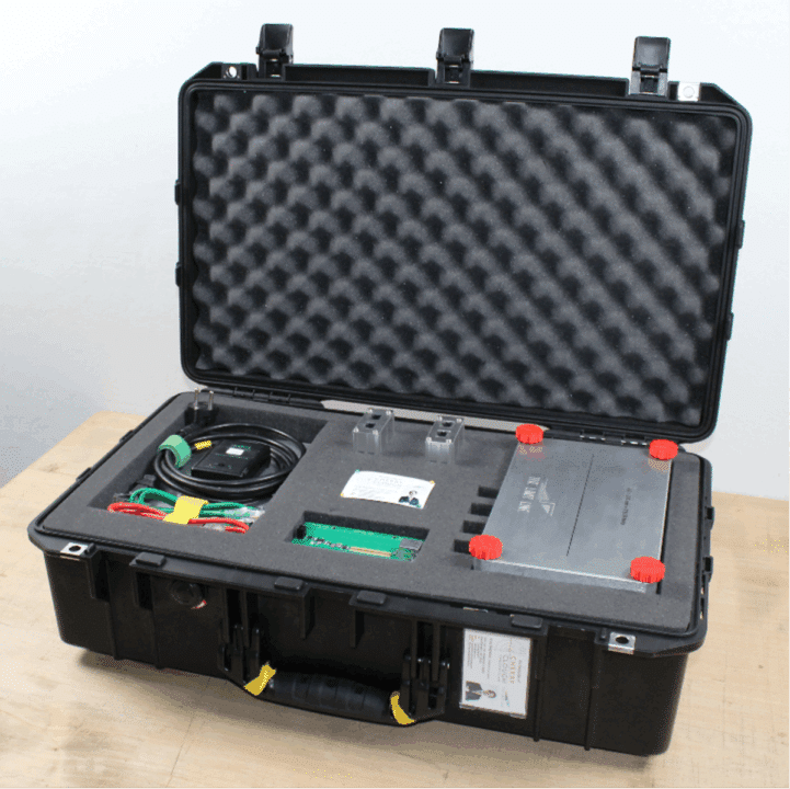
Secondly, the EMD1 is developed so it can be used in a non-EMC-lab environment, saving money on very expensive spectrum analyzers or even more costly test chambers. It doesn’t need a shielded environment or very expensive probes.
Therefore, it can be used in any room — even a conference room — with low-cost near-field probes or current clamps [7].
A cheap PCB antenna can be used for demonstrations of emissions in the far-field, as evaluated by Kenneth Wyatt.
The near-field probes and current clamps can be DIY [7] and used on the EMD1 to learn to debug or test-bench evaluate a product.
Any low-cost spectrum analyzer or oscilloscope with FFT capabilities will do for any demonstration which should be available already.
In addition, it is possible to design your own PCB layout for EMC and evaluate it or compare it against other designs using this EMC Demonstration System.
A very popular and easy-to-perform demonstration is near-field probing apertures and slots — simultaneously training engineers in near-field debugging [6],[7]. Or its overall emissions can be evaluated for different enclosure designs, cable types and mismatching/matching loads.
It can be easily demonstrated that when volumetric shield is interrupted, its overall resulting emissions will be very different as shown in Figure 3.
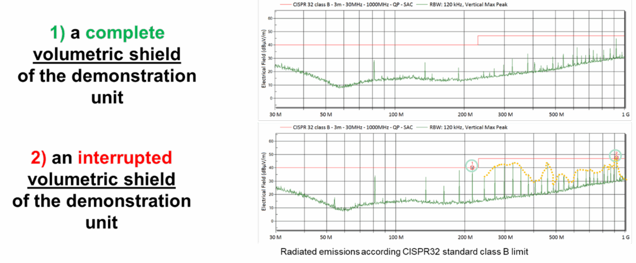
Bottom: resulting radiated emissions according to CISPR32 in case of an interrupted volumetric shield.
Furthermore, the EMD1 is capable of quickly showing the difference in performance of mains filters, such as filters mounted on painted or surface-treated cabinets and enclosures, giving an increased and frequency-dependent RF-bonding impedance between the filter and the overall RF reference.
This yields a reduced attenuation performance over its frequency range.
This principle can be shown simply by a flip of a switch, without the need for costly or time-consuming demonstration set-ups. This is done in a safe setting like a conference room or classroom.
There is no need for expensive EMC test chambers or antennas. It uses a low-cost spectrum analyzer and DIY near-field probes.
The top image in Figure 4 shows the conducted emissions on the mains cable in case of an unfiltered mains, where the bottom image shows the conducted emissions on the mains cable in case of a filtered mains, and this for:
- A “good” ground bond (i.e. low-impedance)
- A “bad” ground bond (i.e. high-impedance)

four possible situations: unfiltered, filtered “bad” chassis bond (i.e. high-impedance), filtered “good” chassis bond (i.e. low-impedance).
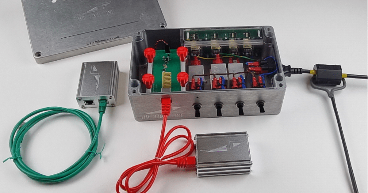
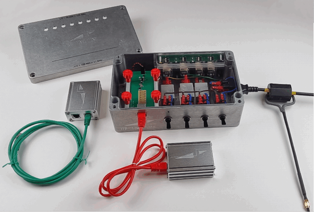
The EMC Demonstration System is an actual product, not a simulator, nor something that looks like a product. It is designed to replicate real life [3].
Besides system-level EMC demonstrations, the smart PCB clamping system can be fitted with various LVDS driver PCBs.
The difference in conducted and radiated emissions can be quickly shown for PCB designs that have the same BOM and differ only in their layout. One of the variants is shown in Figure 5 below.
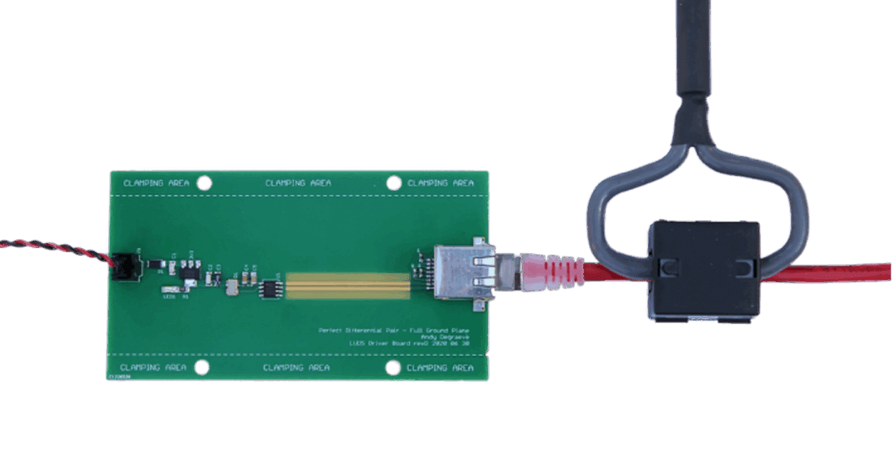
Any poor application of one of the good PCB design practices for EMC can be quickly seen.
Different types of modern cables can be connected, e.g., shielded or unshielded, and their conducted and radiated emissions can be evaluated.
These cables can be terminated in a matched or mismatched load, and this in a shielded or unshielded connecter, enabling the user to quickly play around with volumetric shielding and/or sniffing for leakages.
At university, last year Master of Science in Electronics and ICT Engineering Technology students were first taught a two-hour class on how to use a CAD tool for PCB design. They had to design the same PCB twice.
First, without any prior knowledge of PCB design and layout techniques for good EMC. Afterwards, they were taught only five PCB design techniques for good EMC, and they had to lay out the same high-speed PCB with this ‘new understanding.’
No changes in layer stack-up nor any changes in the BOM were allowed — they only ‘moved around the copper patterns.’
Then they had to evaluate the EMC of both designs against each other.
Figure 6 and Figure 7 below show their evaluation of both PCB versions. In this case it was tested against the CISPR32 radiated emissions class B standard.
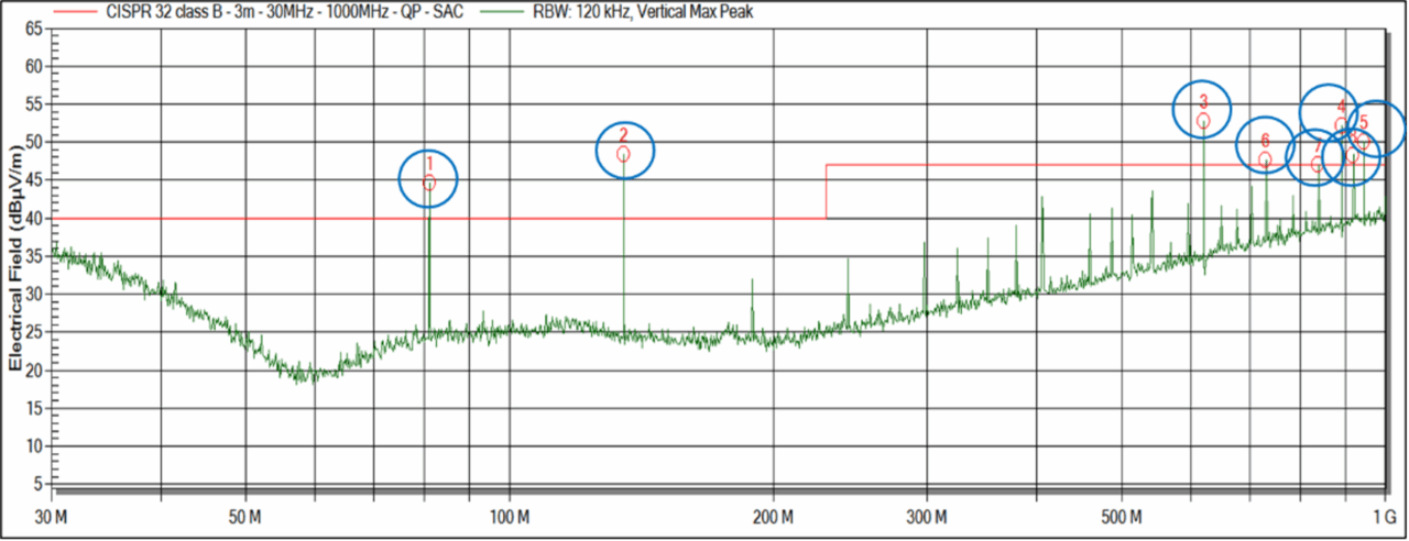
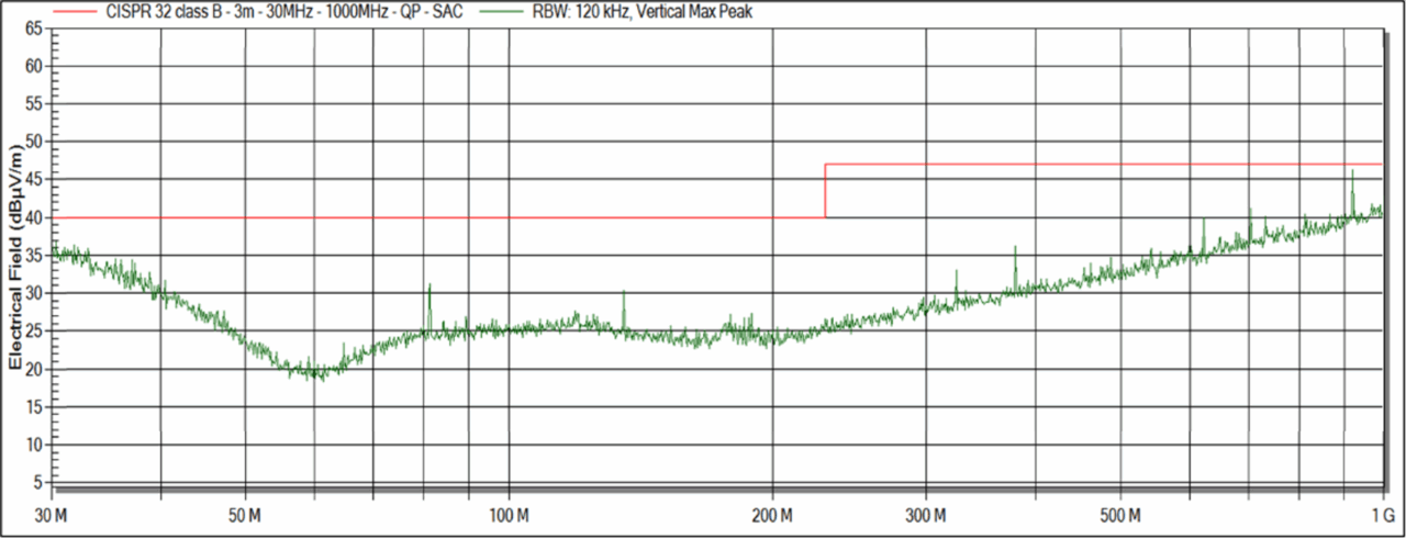
Of course all students were baffled with the difference in emissions, although both PCBs had the same schematic, identical BOMs and no changes were made in the layer stack-up.
All these good EMC engineering practices and techniques and much more are also covered in the training courses that we offer, where I train engineers into the state-of-the-art design techniques for good EMC [4]-[7].
These courses are updated three to four times a year to stay current.
SUMMARY
With this EMC Demonstration System, you can:
- Teach and train your engineers or students
- Educate managers in EMC in a very visual manner
- Demonstrate major EMC phenomena
- Learn the distinction between good and bad EMC practices
- Visualize different EMC phenomena (conducted and radiated)
- Prove EMC fixes (filters, ferrites, gaskets, etc.)
- Show the influence of different PCB designs on EMC, especially the benefits of good PCB layout techniques
- Teach EMC debug and diagnostic methods using both low-cost (DIY) and current probes, and small antennas.
Using this tool has saved companies vast amounts of money, helping them achieve the lowest possible BOM cost and the fastest time-to-market. It is the tool to bridge the gap between theory and practice.
REFERENCES
- Andy Degraeve, Tim Claeys, Filip. Vanhee, Joan Peuteman, Davy Pissoort and Keith Armstrong, “Development of an EMC demonstration unit,” 2016 International Symposium on Electromagnetic Compatibility – EMC EUROPE, Wroclaw, Poland, 2016, pp. 422-427, doi: 10.1109/EMCEurope.2016.7739177.
- Andy Degraeve, Joan Peuteman, Davy Pissoort, Keith Armstrong, “Teaching EMC using an EMC demonstration unit,” 2018 IEEE International Symposium on Electromagnetic Compatibility and 2018 IEEE Asia-Pacific Symposium on Electromagnetic Compatibility (EMC/APEMC), Suntec City, Singapore, 2018, pp. 1255-1260, doi: 10.1109/ISEMC.2018.8393990.
- Andy Degraeve, “EMC Demonstration System – Teach, Train and Bridge the Gap between EMC Theory and EMC Practice.” EMC Demonstration System, 2025, [online] Available: http://www.thelimitline.com/emc-demonstration-system.
- Andy Degraeve & Keith Armstrong, “Essential PCB design/layout techniques for quick and cost-effective SI, PI, EMC”, EMC Education and Training, 2025, [online] Available: https://www.thelimitline.com/emc-education-and-training.
- Andy Degraeve & Keith Armstrong, “Advanced PCB design/layout techniques for quick and cost-effective SI, PI, EMC”, EMC Education and Training, 2025, [online] Available: https://www.thelimitline.com/emc-education-and-training.
- Andy Degraeve & Keith Armstrong, “Good EMC engineering practices for equipment, systems and installations”, EMC Education and Training, 2025, [online] Available: https://www.thelimitline.com/emc-education-and-training.
- Andy Degraeve & Keith Armstrong, “Low-cost, quick, benchtop EMC testing helps de-risk all project stages”, EMC Education and Training, 2025, [online] Available: https://www.thelimitline.com/emc-education-and-training.