Understanding EMC is all about two important concepts: (1) all currents flow in loops and (2) high frequency signals are propagated as electromagnetic waves in transmission lines and the field energy travels through the dielectric. The two concepts are related because they are intertwined together. Digital signals create the propagating field, which induces the convection current to flow in the copper traces/planes.
CURRENTS FLOW IN LOOPS
These two concepts are closely related and coupled to one another. The problem we circuit designers miss is defining the return path back to the source. If you think about it, we don’t even draw these return paths on the schematic diagram – just showing it as a series of various “ground” symbols.
So what is “high frequency”? Basically, anything higher than 50 to 100 kHz. For frequencies less than this, the return current will tend to follow the shortest path back to the source (path of least resistance). For frequencies above this, the return current tends to follow directly under the signal trace and back to the source (path of least impedance).
Where some board designs go wrong is when high dV/ dt return signals, such as those from low frequency DCDC switch mode converters or high di/dt return signals get comingled with I/O circuit return currents or sensitive analog return currents. We’ll discuss PC board design in the next article. Just be aware of the importance of designing defined signal and power supply return paths. That’s why the use of solid return planes under high frequency signals and then segregating digital, power, and analog circuitry (keeping them separate) on your board is so important.
HOW SIGNALS MOVE
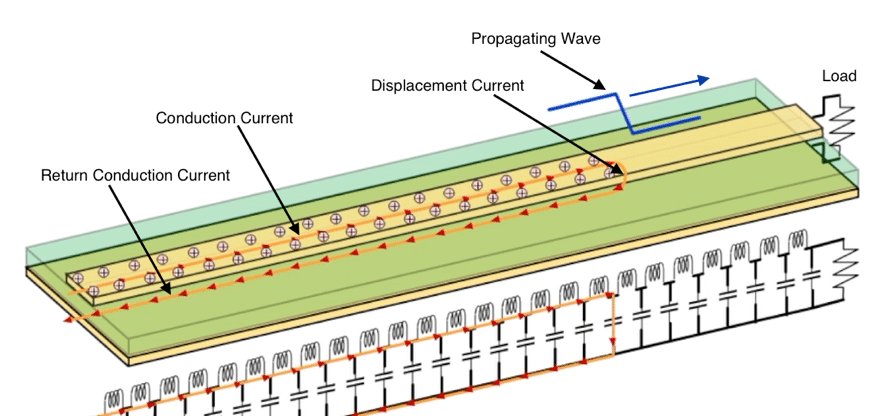
At frequencies greater than DC, digital signals start to propagate as electromagnetic waves in transmission lines. As shown in Figure 1, a high frequency signal propagates along a microstrip transmission line (circuit trace over return plane, for example), and the wave front induces a conduction current in the copper trace and back along the return plane. Of course, this conduction current cannot flow through the PC board dielectric, but the charge at the wave front repels a like charge on the return plane, which “appears” as if current is flowing. This is the same principle for capacitors and Maxwell called this effect “displacement current”.
The signal’s wave front travels at some fraction of the speed of light, as determined by the dielectric constant of the material, while the conduction current is comprised of a high density of free electrons moving at about 1 cm/ second. The actual physical mechanism of near light speed propagation is due to a “kink” in the E-field, which propagates along the molecules of copper. Refer to References 1, 2, and 3 for further details.

Figure 1 – A digital signal propagating along a microstrip with currents shown.
The important thing is that this combination of conduction and displacement current must have an uninterrupted path back to the source. If it is interrupted in any way, the propagating electromagnetic wave will “leak” all around inside the PC board dielectric layers and cause electromagnetic coupling and “common mode” currents to form, which then couple to other signals (cross-coupling) or to “antenna-like structures”, such as I/O cables or slots/apertures in shielded enclosures.
Most of us were taught the “circuit theory” point of view and it is important when we visualize how return currents want to flow back to the source. However, we also need to consider the fact that the energy of the signal is not only the current flow, but an electromagnetic wave front moving through the dielectric, or a “field theory” point of view. Keeping these two concepts in mind just reinforces the importance of designing transmission lines (power and signal traces with return path directly adjacent), rather than just simple circuit trace routing.
It is very important to note that all power distribution networks (PDNs) and high frequency signal traces are transmission lines and the energy is transferred as electromagnetic waves at about half the speed of light in normal FR4-type board dielectrics. We’ll show what happens when the return path or return plane is interrupted by a gap in the next article. More on PDN design may be found in Reference 4, 5, and 6.
DIFFERENTIAL MODE VERSUS COMMON MODE CURRENTS
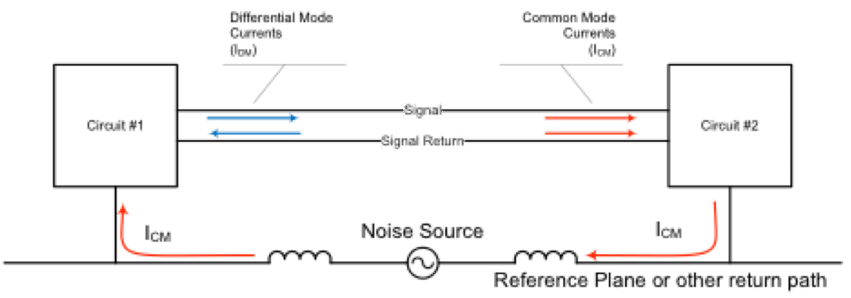
Referring to Figure 2, the differential mode current (in blue) is the digital signal itself (in this case, shown in a ribbon cable). As described above, the conduction current and associated return current flow simultaneously as the signal wave front moves along the transmission line formed by the microstrip and return plane.
The common mode current (in red) is a little more complex in that it may be generated in a number of ways. In the figure, the impedance of the return plane results in small voltage drops due to multiple simultaneous switching noise (SSN) by the ICs. These voltage drops induce common noise currents to flow all over the return (or reference) plane and hence, couple into the various signal traces.

Figure 2 – An example of differential and common mode currents.
Besides SSN, common mode currents can also be created by gaps in return planes, poorly terminated cable shields, or unbalanced transmission line geometry. The problem is that these harmonic currents tend to escape out along the outside of shielded I/O or power cables and radiate. These currents can be very small, on the order of μA. It takes just 5 to 8 μA of current to fail the FCC class B test limit.
SUMMARY
To summarize product design for EMI compliance, a properly designed PC board with adjacent return planes to all signals and PDNs, properly bonded I/O cable shields, well bonded shielded enclosures with minimal slots or gaps, and common mode filtering on all I/O and power cables for unshielded products is generally required for best EMI performance. Paying attention to these factors early in the design greatly reduces the risk of EMC and EMI compliance failures.
REFERENCES
- Bogatin, Signal Integrity – Simplified, 3rd edition, Prentice-Hall, 2018.
- Morrison, Grounding and Shielding – Circuits and Interference, Wiley, 2016.
- Morrison, Fast Circuit Boards – Energy Management, Wiley, 2018.
- Smith and Bogatin, Principles of Power Integrity for PDN Design, Prentice-Hall, 2017.
- Sandler, Power Integrity – Measuring, Optimizing, and Troubleshooting Power Related Parameters in Electronic Systems, McGraw Hill, 2014.
- Novak and Miller, Frequency-Domain Characterization of Power Distribution Networks, Artech House, 2007.


