 The number of RF systems available for use in mission specific aircraft has grown dramatically over the last few decades, with numerous systems operating across very wide bandwidths (some covering almost the entire 1MHz to 40GHz range).
Compatibility issues have become almost a certainty on all but the simplest of aircraft installations, and numerous mitigation techniques have been developed to address these issues. These compatibility issues include:
1. Passive Intermodulation (PIM) incident power on these structures.
2. IF interference, where the transmitter is at the receiver IF frequency.
3. Harmonic interference, where a harmonic of the transmitter is at the intended receive frequency.
4. Cross modulation interference, where a high level transmission close to the receiver frequency is not sufficiently attenuated by the receiver input filter (if any). Here compression, intermodulation and spurious responses can occur in the receiver.
5. Adjacent channel interference from a transmitter close enough to lie within either the receiver IF bandwidth or the receiver bandwidth.
6. Broadband noise from a transmitter which is in band for a receiver.
This paper explains some of the mitigation techniques that can be used to improve intersystem compatibility on an aircraft installation.
PRELIMINARY EMC PREVENTION
Improving intersystem compatibility begins at the initial design stage. When choosing on-board systems, careful consideration should be given to the transmit and receive frequencies of the desired equipment as well as the output power levels, sensitivity levels, blanking capabilities, and intended usage.
A table of all systems and relevant information should be prepared, and this table can be used to determine potential conflicts and the possibility of Simultaneous Operations (SIMOPS). It is important to consider intended usage as some conflicts are quite acceptable. For example the emergency locator transmitter (ELT) transmits in the same range as regular communication radios, however the ELT will only be used in the case of a downed aircraft, and under those circumstances many of the other systems will not be required to operate.
For systems that are required to operate in the same or similar bandwidths, the primary preventative measure is antenna placement. Conflicting system antennas can be mounted at opposite ends of the aircraft or in some cases at the top and bottom of the aircraft. This reduction in coupling increases the isolation between the antennas. The coupling around an aircraft is typically a composite of reflections from the Wings and Engine Nacelle as well as the coupling due to the creeping wave around the fuselage. Various techniques, including measurement and computer modeling, are available to determine the coupling between antennas mounted at various locations around an aircraft. These techniques are described in more detail in references 1 and 2 and in practical terms allows an EMC engineer to decide if it is worthwhile to re-position two co-located antennas to the top and bottom of a fuselage or wing or increase the distance between them.
Effective reduction in coupling may be achieved for horizontally polarized transmitting antennas which operate over a narrow frequency range and which couple to either a vertically or horizontally polarized receiving antennas in close proximity. The location of the two antennas may be chosen so that the direct wave and the wave reflected from the surface of the aircraft tend to cancel. This cancellation may be more effective than locating antennas on opposite sides of the fuselage at low frequency.
Many pieces of equipment also include blanking capabilities. For example, a transmitter may provide a DC output signal when transmitting, and this DC output can be used to disconnect receiving signal paths of local sensitive equipment. Similarly some equipment includes blanking input connections which disconnect the received RF signal when a DC level is present at the blanking input.
ABSORBER
Absorber can also be placed on surfaces, such as the wings, engine, vertical stabilizer and tail plane to reduce reflection as well as for damping surface waves. The absorber may be flexible silicone rubber lossy sheet which is weather proof and can glued to surfaces.
These are typically effective at microwave frequencies, such as used by radar, with some frequency tuned and others effective over a broad band of frequencies. Also a thin ceramic ferrite absorber is available effective from 10MHz to 1GHz. One manufacturer is Cuming Corporation.
FILTERS
The use of low pass, band pass and band stop filters at the input of receivers can be effective at reducing compression, generation of spurious response, and desensitization of the receiver. High power filters are commercially available for use at the output of transmitters and these are used to reduce harmonics and broad band noise from the transmitter.
For transceivers it is possible to design an input filter which can transmit the output power safely and without excessive attenuation.
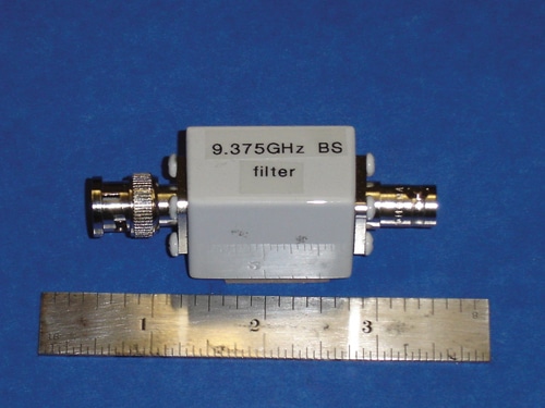
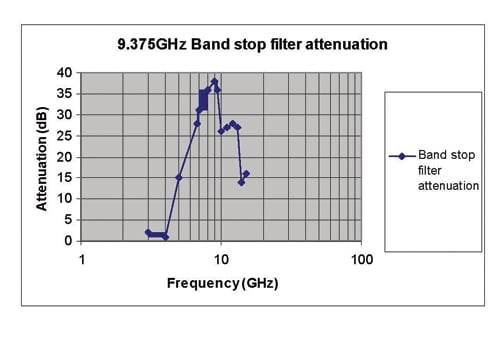
As an example a weather radar transceiver or a SLAR system operating at 9.375 GHz may cause interference to adjacent receivers, and these receivers can be protected using a band stop filter centered at 9.375 GHz. The insertion loss for this filter is negligible at frequencies below 2GHz. The attenuation characteristics of this filter is shown in figure 1. EMC Consulting have designed, built a band stop filter tunable from 700MHz to 1.1GHz with 30dB of attenuation at the center frequency. With the center frequency of this filter adjusted to 1GHz the insertion loss for the filter is less than 0.5dB up to 300MHz and 2dB up to 400MHz. All of the filters described in this report will fit into the small enclosure shown in figure 2 and have been constructed and tested with either BNC or TNC connectors. This size is ideal for connecting directly at the input of the receiver.

Low or high pass filters can be used where one transmitter frequency comes close to, but does not overlap a receiver. For example a receiver operating in the 1 to 30MHz range would benefit from a low pass filter which attenuates above 30MHz when used in close proximity to a transmitter operating in the 30 MHz to 88MHz range.
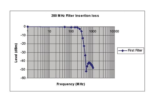
Low pass filters are also effective when the interfering signal is at a significantly higher frequency than the in band receiver frequencies. The performance of a range of these filters is shown in table 1 and for the 200MHz in the plot of figure 3.
Filters with sharper roll off above the upper frequency are available commercially but are typically larger then the enclosure seen in figure 2.
LIMITER
Limiters can be used in conjunction with other mitigation techniques or alone. If a high level signal is being received at the input to a receiver either in band or out of band a limiter can be used to reduce the input level to an acceptable level without interfering with the desired received signal, unless the two are tuned to exactly the same frequency.
For example, a receiver which is sensitive to –50 dBm but which compresses when an out of band signal exceeding 0 dBm is applied may compress when placed in close proximity to a high power transmitter. The introduction of a 0 dBm limiter would reduce the high power received levels to a manageable level while allowing the intentional received levels to pass without compression. The insertion loss for a typical limiter is -2dB from 50 – 500MHz with a useful frequency range of 5 to 3000MHz. EMC consulting has manufactured a PCB on which the limiter was mounted and placed in the enclosure shown in figure 2. The input voltage is 28V and the limiter is protected against all of the EMC power line conducted susceptibility and power characteristics specified in DO-160 or MILSTD-461 by additional components mounted on the PCB. The operating temperature range of the limiter and associated components is -54°C to 85°C.
RF SWITCH AND BLANKING
When transmitters have blanking outputs and receivers blanking inputs then these may be connected to blank the receiver when the transmitter is operational. Some additional components may be required to make the control signal levels compatible. Also when the RF output of the transmitter remains powered up broadband noise is still transmitted. If the transmitter has a blanking output but a receiver does not have a blanking input an RF switch may be used at the receiver input. One such switch is the Mini-circuits ZFSWA-2- 46 which can be used from DC-4.6GHz. It has maximum 0.8dB attenuation from DC-200MHz, 1.3dB up to 1GHz and 2.6dB from 1- 4.6GHz. It requires two signal inputs to switch from “off “ to “on”, -8V on one and 0V on the other or vice versa. It is possible to use a simple sine wave oscillator connected to the +28V power, transformer, rectifier and linear regulator to obtain the –8V and the circuit can be protected against all of the DO-160 or MIL-STD 461 power line conducted susceptibility test levels. The maximum input level for this switch is +24dBm and the video leakage (the control level feedthrough conducted out of the RF output) is 30mV pk-pk.
DELAY AND PHASE SHIFT CANCELLATION
The concept of in band cancellation is introduced in section 10.2.2.2 of reference 3. When the transmit and receive frequency bands overlap then filters are clearly not applicable.
When the interferer received level is extremely high and may result in damage to the receiver the limiter may be used. However even with the limiter in circuit the level after limiting may be high enough to result in receiver de-sensitization, cross modulation or spurious generation.
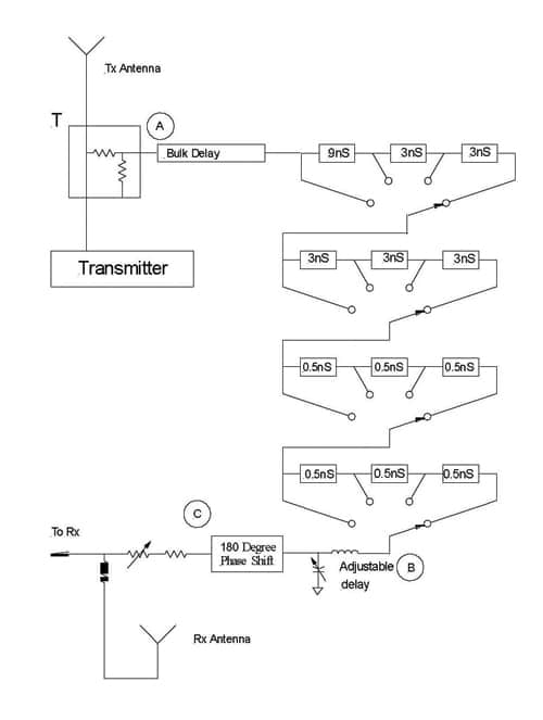
To cancel or reduce the interferer level a propagation delay, 180 degree phase shift and summation circuit has been developed. This is shown in the block diagram figure 4. The output of the transmitter is tapped off with no reduction in power level between the transmitter and antenna. This can be achieved anywhere on the transmit cable from the transmitter end to the transmit antenna end. The ideal location depends on the total propagation delay of the transmit cable, the coupling path in air between the antennas and the receiver cable, as described later.
The output of the transmitter is attenuated and matched to the impedance of the cable which connects to the circuit at point A. The interferer signal is then passed through a bulk delay. The bulk delay can be in the tens of microseconds the only limit is the attenuation inherent in the delay elements and the physical size of the enclosure. In practice delays up to 500nS are adequate. For the final selection of the total delay thin film delay lines can be connected in or out of circuit and a fine tuning performed with a variable capacitor and an inductor. With 0.5nS, and 3nS thin film delay circuits the selectable delay can be from 0.5nS to 18nS in 0.5nS increments and the tuned delay can be adjusted over 0.5nS. The total transmitter to circuit cable delay, bulk, and variable delays are chosen to be exactly equal to the transmitter to receiver total path propagation delay. This means that the input signal to the circuit from the receiving antenna and the signal at location B in the circuit are in phase. The signal at point B then undergoes a 180 phase shift which is virtually frequency independent.
The signal at point C is then adjusted in level and summed with the receiver input signal.
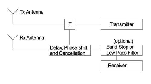
This achieves an almost complete cancellation at a specific frequency. At either side of this frequency the amplitude at the output of the delay circuit is different from the receiving antenna level. This is because the attenuation with frequency of the transmitter to receiver path is different from the phase shifter cancellation circuit. As the intentional signal from the receiving antenna is routed through the circuit the attenuation of the signal is 1.8dB. Figure 5 shows the path between transmitter and receiver. An input filter is shown in figure 5 but is not necessary.
The transmit path propagation delay can be determined approximately by transmitting a pulse amplitude modulated RF from a signal generator, using the modulation pulse to trigger an oscilloscope, and measuring the delay. An external modulator or RF switch may be used if the generator does not allow pulse modulation. The fine tuning of the delays in the circuit can be accomplished by again using a pulse amplitude modulated signal and comparing the output of the circuit to the input of the receiver. The two channels of the scope used to measure the two signals must have no delay between them (chopped display may be required).
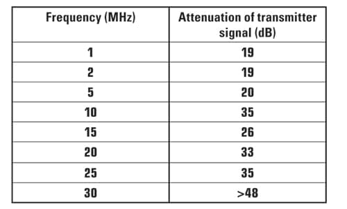
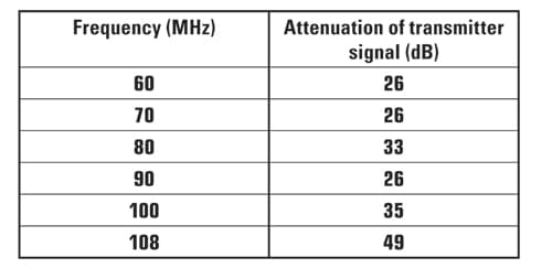
The circuit was adjusted and tested from 1MHz to 30MHz, with the maximum attenuation adjusted at 30MHz. The attenuation achieved is shown in table 2. With the circuit adjusted for 108MHz the attenuation from 60MHz to 108MHz is shown in table 3.
At a single frequency such as 152MHz the cancellation can result in an attenuation of 28dB.
The delay circuits within the phase shift and summation circuit have some temperature coefficient as does the permittivity of the transmit and receive cables and this changes the delay. However the measured change in attenuation of the delay and cancellation circuit was only 1.5dB from 4°C to 47°C.
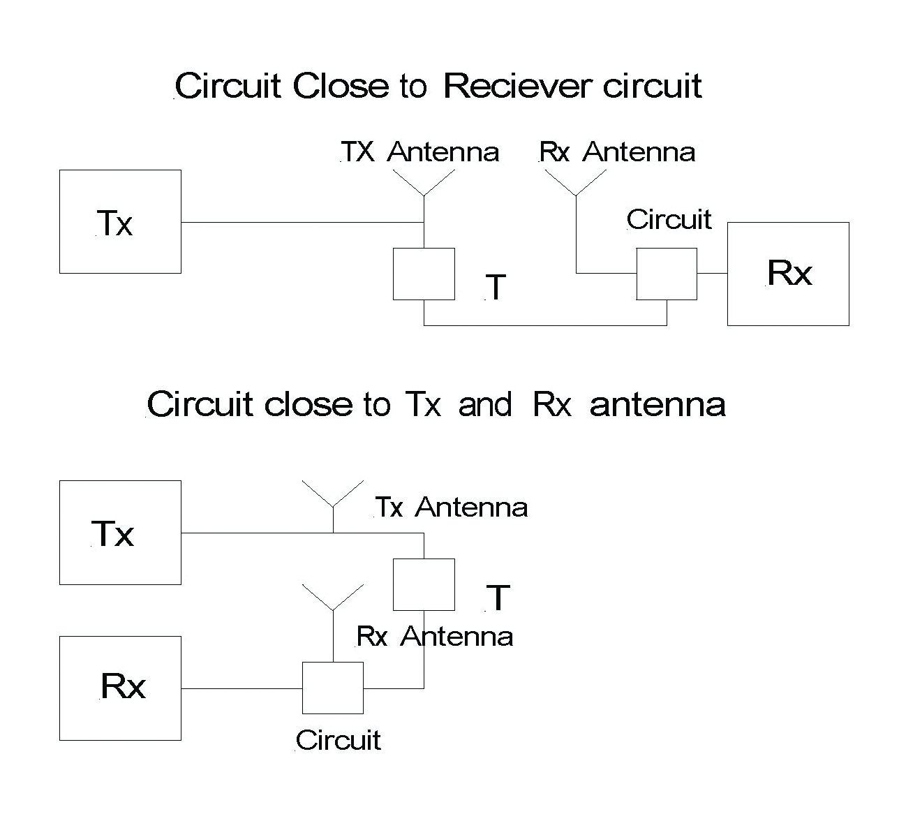
The location of the T and the circuit depend on the location of the transmitter, receiver, transmit antenna and receive antenna. The goal would be to reduce the amount of cable delay and therefore the amount of bulk delay required in the circuit. Two possible configurations are shown in Figure 6.
REFERENCES
[1]. D. Weston. “Antenna to Antenna Coupling on an Aircraft Using a 1/10th Scale Model with Results Compared to the FEKO Electromagnetic Analysis Program,” EMC Europe 2010, Wroclaw, Poland.
[2]. D. Weston. “Comparison of Techniques for Prediction and Measurement of Antenna to Antenna Coupling on an Aircraft,” EMC Europe 2011, York, England.
[3]. D. Weston. “Electromagnetic Compatibility: Principles and Applications,” Second Edition. 2001. Marcel Dekker Inc, New York.
David A. Weston is principle EMC engineer at EMC Consulting, Inc., Merrickville, Ontario, Canada. A member of IEEE and NARTE, Weston has worked full time in EMC for the last 30 years. He is author of the book, “Electromagnetic Compatibility: Principles and Applications” as well as numerous papers and reports, many of which are available at emcconsulting.com. He studied at Croydon Technical College from 1960 to 1965.
