Robert J. Vermillion, RMV Technology Group, LLC, NASA-Ames Research Center, Moffett Field, California USA; Doug Smith, DC Smith Consultants, Los Gatos, California, USA
For years, semiconductor and aerospace engineers have fielded questions regarding the suitability of using gelatinous and tacky coated packaging materials for the distribution, storage, and sale of ESD sensitive devices. Since this type of packaging is often utilized for ESD sensitive devices on an ANSI/ESD S4.1-2006 ESD work surface without ionization, the question arises: Does the practice of anchoring components without requiring specially designed packaging or ionization constitute a compliant method in protecting Ultrasensitive Class 0 ESD devices?1
The author’s intent is to analyze gelatinous and tacky coated technologies for compliance within a static controlled environment or ESD Protected Area (EPA). Two product carrier types, a cross-link gelatinous polymer insert (Figure 1) and a coated polymer insert with static dissipative properties (each used in conjunction with tweezers for manual pick and placement) were selected for test and evaluation.
Background
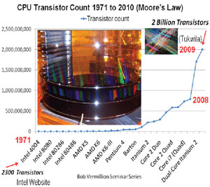
To gain a better understanding of potential risks associated with the use of inadequate packaging within an ANSI/ESD S4.1-2006 or MIL-PRF-87893B-1997 protective ESD work station, one needs only to compare today’s technology miniaturization to 1969 when Apollo 11 landed on the moon. In May 2011, Astronaut Col. Buzz Aldrin, Ph.D. stated that a hand held smart phone has more processing power than NASA’s Apollo 11 computer. In 1971, the Intel 4004 microprocessor was 2300 transistors equivalent. Now, according to Processor News, Intel’s CPU breaks the 2 billion transistor barrier with the Tukwila (Reference Illustration 1).
As technology has progressed from ferrite cores, to individual transistors, to billions of transistors, the ESD sensitivity of these devices has increased exponentially. The relative robustness of devices with ESD sensitivities of 1000 volts in the early 80s has been replaced with device threshold below 50 volts today. The disk drive sector’s GMR, (giant magnetoresistive), PMR (perpendicular magnetic recording), TMR (tunneling magnetoresistive), and HAMR (heat assisted magnetic recording) generally identified as EAMR (Energy Assisted Magnetic Recording) heads are known for ESD sensitivity at <5 volts for the past five years or more. Today HBM sensitivity is about 1 volt. Increasing the necessity of protecting devices from ESD events at these low levels will ensure both yield and reliability.
Because of increased device sensitivity, in-process packaging and handling materials should be capable of offering the aerospace & defense, semiconductor, medical device, disk drive and automotive community protection from electrostatic discharge by meeting the requirements called out in ANSI/ESD S541-2008. Section 7.0 – Classification of ESD Packaging Material Properties that states:
Materials and packages useful in preventing damage to sensitive electronic devices exhibit certain properties that include:
• Low Charging (antistatic)
• Resistance:
-Conductive
-Dissipative
-Insulative
• Shielding:
-Electrostatic Discharge
-Electric-field
Methodology and Test Results
As previously stated, two products were evaluated for suitability in an EPA Class Zero ESD workstation. Product A is a cross-linked gelatinous polymer package insert. According to the supplier claims, Product B is a tacky static dissipative coating property independent of the conductive surface below. Both the gelatinous polymer and tacky surface coating, hold devices in place either upside down or horizontal to a work station and require minimal effort for physical removal of the devices from the packaging.
In this article, the battery of ESD tests represents a snapshot of what is required for compliance to a formalized materials qualification process. The following testing methods were utilized to determine the ESD safe performance of the packages:
1. Surface Resistance (ANSI/ESD STM11.11) at 12%+/-3%RH
2. Volume Resistance (ANSI/ESD STM11.12) at 12%+/-3%RH
3. Electrostatic Decay; Gelatinous/Tacky inserts to Ground [MIL-STD-3010B (Modified),12%+/-3%RH]
4. Faraday Cup testing per ESD adv.11.2 at 12%+/-3%RH
5. Peak Voltages of Products A and B inserts at 12%+/-3%RH after Charge and Grounding
6. Contact Discharge of Tweezers making intimate Contact with an ESD Sensitive Device after 1kV charging at 30%RH.
a. Current Probe
i. with ionization
ii. without ionization
Surface and Volume Resistance versus Relative Humidity (RH)

It is a misconception to assume that ESD testing at low and high relative humidities will produce similar measurements. Arguably, this may be true for humidity independent technologies, but materials that rely upon moisture to facilitate electrical conductivity such as antistatic polymers may produce significantly different readings at 50% RH in comparison to ESD testing at 12% RH. Many organizations maintain 30%RH to 70%RH within an EPA.
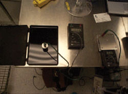
In accordance with ANSI/ESD STM11.11-2006 and ANSI/ESD STM11.12-2007, Products A and B were preconditioned at 12% +/-3% RH and 730F +/-50F for 48 hours prior to testing. Figure 2 illustrates Product A undergoing Surface Resistance testing; Figure 3 illustrates Volume Resistance testing for Product B. Products A and B surface resistance measurements are benchmarked in Table 1.

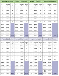

For Product A, the exterior carbon loaded rigid plastic cases measured in the lower static dissipative range. Product B produced conductive readings (Table 1) for said cases. Both cases are suitable for use in an EPA. Since the components make intimate contact with Products A and B substrates, a carbon case would not represent a CDM hazard. As illustrated in Table 2, the gelatinous-like substrate of Product A measured above the threshold of <1.0 x 10¹¹ ohms for an average or 3.2 x 10¹² ohms (failed); Product B findings, however, were in the static dissipative range for an average of 4.5 x 10⁵ohms (passed).

Volume Resistance testing is important as it represents a package’s ability to maintain continuity when placed atop a grounded work station. In Product A, a charged gelatinous surface (despite being grounded) could represent an ESD hazard when stainless steel tweezers make contact with ESD sensitive devices.
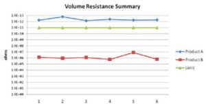
Product A Volume Resistance (Table 3) average measured insulative at 2.6 x 10¹² ohms (failed). Product B, however, measured static dissipative at 2.2 x 10⁶ ohms (passed).
Electrostatic Decay per Mil-STD-3010B-2008 (Modified)

Electrostatic Decay
This test method measures the rate of decay of a charged isolated object to 10 percent of its original value. Mil-STD-3010B specifies that the charged object at +/- 5000 volts should drain the voltage to +/- 500 volts or lower. For several years, a common voltage range of +/-1000 volts to +/-100 volts has been utilized. A decay time of less than 2.0 seconds is called out in MIL-PRF-81705E and the former EIA-541 as passing. This test represents a material’s ability to dissipate induced voltage with proper grounding. Decay tests have difficulty with materials of complex construction such as ESD convoluted foams, vacuum-formed polymers and small items that could fall below the measuring range of the testing equipment’s fixturing.
For Product A, the test was stopped (see Figure 4a, left) after 3 seconds. Product B (see Figure 4a, right), however, facilitated electrostatic decay through the grounded polymer insert and carbon case on top of a charge plate. Even after grounding for 5 seconds, the Product A gelatinous insert substrate did not bleed off charge (see Figure 4b). The plate voltage remained at 1023.8 volts and -1023.6 volts respectively. It should be noted that when the charge plate voltage reaches +/-1000 volts, a decay timer will start.


Product A overlaps in Table 6 and is above the limit of <2.0 seconds. Product B, however, passed as illustrated in table 6.
Faraday Cup (Q=CV) per ESD Adv. 11.2
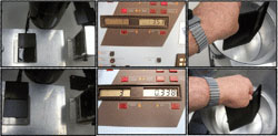
After 48 hours of preconditioning at 12%+/-3%RH in the test chamber, Products A and B were placed under an ionizer that was balanced to less than 10 volts. Ionization removed potentially stored charges prior to Faraday cup testing. Then, the products were placed on a charge plate set at 1000 volts. The packages were removed from the plate, grounded for a period of 5.0 seconds and allowed to free fall into a Faraday Cup as illustrated in Figure 5. Some organizations require a passing score of <+/-1.0 nC that is about <+/-100 volts. Table 7 illustrates the results of testing for Products A and B. Product A failed the test. Product B passed the test and was within the acceptance limits.


Table 8 illustrates the Faraday Cup results. The green and purple lines exhibit the upper and lower limit of +/-1.0nC. Product A results are illustrated by a blue line and Product B is illustrated with a red line. Product B passed the test.


Non Contact Voltage Testing
The technique of pinpointing hidden charges (hot spots) is accomplished by the use of a non-contact voltage measurement device as illustrated in Figure 6. It is important to test for hot spots since an ESD sensitive device could be placed over this area and damaged by tweezer removal. If the overall surface measures <50 volts and one spot peaks out at 200 volts, this could represent a potential hazard to a 100 volt ESD sensitive device with tweezer contact. Product A peak voltage surpassed the range of the non-contact voltage system at -1023.5 volts. Product B peaked at -30 volts.
Contact Discharge Measurements with and without Ionization using Tweezers:

Conducting Contact Discharge Measurements “with and without” Ionization:
Both Products A (glossy looking insert) and B (satin appearing insert) were placed on a charge plate with a US quarter atop the packaging inserts. Under ionization, Product A was neutralized to remove charge. A 6” x 6” 20pF charge plate was then charged to 1000 volts. A grounded person makes intimate contact with the quarter and then grounds the charge plate. This simulates a grounded operator at an ANSI/ESD S4.1 workstation making intimate contact with stainless steel tweezers and an ESD sensitive device. If charge is in proximity to an ESD sensitive device, contact between metal to metal surfaces could produce an electrostatic discharge.
An F-65 current probe is positioned over the quarter and grounded stainless steel tweezers made contact with the coin (see Figures 7 and 10). In the left-hand section of Figure 8, illustrating charge on the plate, note the dip when a quarter was touched after said plate was charged to 1000 volts. This finding is due to the capacitance between the quarter and the now grounded quarter (after being touched by a person wearing a grounded wriststrap.

Product A produced a remarkable discharge curve as illustrated in Figure 8. In this case, the discharge current was 4.4 Amperes (vertical scale on the scope screen was 1 Amp/div and horizontal scale was 2 ns/div) with a sub-nanosecond risetime and about 2.0 ns pulse width. Six separate discharges were measured that ranged from about 3.0 Amperes to 4.4 Amperes peak. Ten years ago it would take 20mA lasting one nanosecond to kill a disk drive head.

In the case of Product B, as illustrated in Figure 9, touching the quarter by the grounded person, initiated a passing charge decay of the plate (see Figure 9 – Left). Consequently, there was no resulting discharge when the quarter was touched by stainless steel tweezers inserted through the current probe. This test was repeated six times with no discharge current recorded. Note, the vertical scale on the scope was only 100 mA/div, 10 times more sensitive than Figure 8, with a trigger level of less than 20 mA and yet still no discharge was recorded. Therefore, Product A could pose a hazard during placement and removal of ESD sensitive devices from the gelatinous type surface while Product B did not produce a discharge.
Product A with Ionization
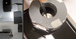
Figure 10 illustrates the tweezers being inserted through the current probe.

Figure 11 illustrates a small discharge current waveform of about 70 mA that occurred on four of six attempts. For two attempts, no discharge was recorded. Notice on the left side of Figure 11 how the ionization slowly discharged the charged plate over a few seconds so that little or no discharge occurred when the quarter was touched by the tweezers.

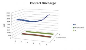
Under ionization, Product A (dark red) produced negligible to no discharges. Product B did not require ionization at 30%RH as illustrated in Figure 11 and Table 10.
Conclusions
In summary, the practice of anchoring components with an attraction mechanism can constitute an ESD compliant method in protecting Ultrasensitive Class 0 ESD devices but only after conducting careful evaluation and qualification of the product.
Product A gelatinous type platform for staging ESD sensitive devices measured insulative and was not in compliance with the ANSI/ESD S541-2008 (ESD Packaging & Materials) standard. Product B’s tacky-like substrate was static dissipative facilitating electrostatic decay and low charging at 12%RH. Without ionization, Product A did not prevent ESD events when conductive tweezers-quarter contact was made. However, Product A, did not pose issues under a flow of Steady State DC ionized air. In contrast, Product B did not require ionization to prevent discharges of an ESD sensitive device. Without considering the insert, both carbon loaded cases were in compliance with ANSI/ESD S541-2008. The supplier should be contacted for the product’s intended application. However, the end user must still validate supplier claims to determine what packaging style is appropriate for use in an ESD Control Area.
Special Acknowledgement
A special thank you to Mr. Brad Alhm, President,Conductive Containers, Inc. in providing samples of Product B (brada@corstat.com).
A special thank you to Melissa Jolliff, Subject Matter Expert in the field of Electrostatic Discharge Mitigation.
References:
[1]. Dr. John Kolyer and Watson, “ESD from A to Z,” 2nd Edition.
[2]. Mil Handbook 1686C-1995.
[3]. Mil Handbook 263B-1994.
[4]. EIA STANDARD (defunct) Packaging Materials Standards for ESD Sensitive Items, EIA-541, June 24, 1988, Appendix C, “Triboelectric Charge Testing of Intimate Packaging Materials”.
[5]. ANSI/ESD S20.20-2007
ANSI/ESD S541-2008
ANSI/ESD S3.1-2006
ANSI/ESD S4.1-2006
ANSI/ESD STM4.2-2006
ANSI/ESD STM11.11-2006
ANSI/ESD STM11.12-2007
ANSI/ESD STM11.13-2004
ESDA Adv. 11.2-1995
[6]. Albert Escusa and Bob Vermillion, “Using An ESD Packaging Materials Qualification Matrix for Contract Manufacturing and Supplier Conformance,” Sep 1, 2006.
[7]. Dr. John M. Kolyer, Ph.D., Rockwell International Telephone interview in 2004.
[8]. John Kolyer and Donald Watson, The Charged Device Model & Work Surface Selection, October 1991, pp. 110-117
[9]. Humidity & Temperature Effects on Surface Resistivity, John Kolyer and Ronald Rushworth Evaluation Engineering, October 1990, pp. 106-110 Military Handbook-263B-1994
[10]. Triboelectric Testing at KSC Under Low Pressure and Temperature ESD Association Proceedings 2002, Dr. Ray Gompf, PE
[11]. ITRS Technical Requirements – Electrostatics, The ITRS is devised and intended for technology assessment only and is without regard to any commercial considerations pertaining to individual products or equipment Intel Website, Moore’s Law
©2011-RMV Technology Group, LLC-All Rights Reserved.
Bob Vermillion, CPP/Fellow, is a Certified ESD & Product Safety Engineer-iNARTE with subject matter expertise in the mitigation of Triboelectrification for a Mars surface and in troubleshooting robotics and systems for the aerospace, disk drive, medical device, pharmaceutical, automotive and semiconductor sectors. A co-author of several ANSI level ESD documents, Vermillion serves on the BoD with iNARTE and is a member of the ESDA Standards Committee. Speaking engagements include ESD Seminars in the United States and abroad and ongoing guest lecturer invitations for California State Polytechnic University, San Jose State University, University of California at Berkeley and Clemson University. In 2011, Vermillion will conduct a Materials/Packaging Seminar for Oxford University. Vermillion is Chief Technology Officer of RMV Technology Group, LLC, a NASA Industry Partner and 3rd Party ESD Materials Testing, Training and Consulting Company. He can be reached at 650-964-4792 or bob@esdrmv.com.
Doug Smith, recently returning from lecturing at Oxford University, specializes in high-frequency measurements, circuit/system design and verification and EMC, among others. Smith’s consulting activities focus on design verification and problems at the system, circuit, and device level as well as EMC and immunity (including ESD) problems. By applying specialized knowledge and measurement technology that he has developed over the years, Smith often solves design or field problems in a much smaller amount of time that could take engineers weeks, months or years of effort using conventional engineering methods of investigation. He can be reached at 408-858-4528 or doug@dsmith.org.
