Abstract
One of the most widespread design defects in automotive printed circuit boards is the lack of an established high-frequency reference ground. This problem is exacerbated by a tendency among automotive design engineers to cut up solid current return planes in an attempt to establish “noisy” and “quiet” grounds.
Introduction
Too often, the designers of automotive electronic systems shoot themselves in the foot (so to speak), making design decisions that ultimately make it difficult for their products to meet the automotive EMC requirements. Basic design flaws such as improper grounding, poor trace routing, and ineffective decoupling are widespread throughout the industry. Many designs also fail to control the routing of currents induced by immunity tests such as bulk current injection or electrical fast transient testing.
Historically, the significance of these design flaws has been diminished by relatively long development cycles that allowed a test-and-fix design strategy. EMC problems that couldn’t be fixed were often dealt with by waiving the requirement. Today however, a growing number of electronic systems play a critical role in automotive safety. There is no opportunity to experiment with multiple iterations of the hardware design during development; and waivers of EMC requirements are becoming harder to obtain.
This article addresses one of the most widespread and damaging design flaws in automotive printed circuit boards today, the lack of a single high-frequency ground reference. More specifically, there is a tendency among automotive circuit board designers to over-partition their “ground” planes.
What’s the Problem?
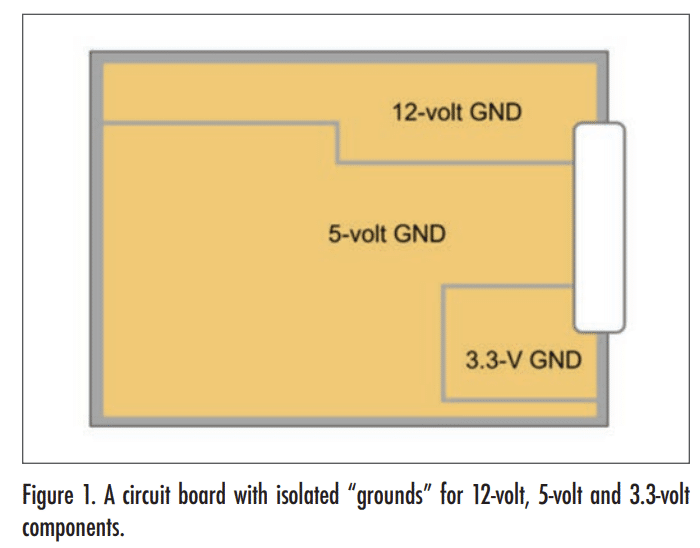
It is not uncommon for an automotive circuit board to have multiple “grounds”. For example, as illustrated in Figure 1, there may be one ground for the 12-volt devices, one ground for the 5-volt devices, and a separate ground for the 3.3-volt digital logic. It is also not uncommon to see isolated grounds for analog sensors, power supplies, motor drivers, memory devices or anything else that is considered particularly noisy or susceptible to noise. Decisions to isolate various grounds are motivated by a desire to reduce interference between various circuits on the board. Usually, this is done without any attempt to quantify the amount of interference that would have resulted if the grounds had not been isolated (even though this is a simple calculation).
The problem with isolating the voltage references (ground) of various circuits on a printed circuit board is illustrated in Figure 2. Isolated grounds are not held to the same potential, i.e. there is likely to be a voltage difference between them. That means there is likely to be a voltage difference between circuits referenced to different grounds. If those circuits communicate with each other on the board, that voltage difference appears as noise on the signals. If those circuits communicate with circuits off the board, then wires leaving the board have a voltage difference between them.
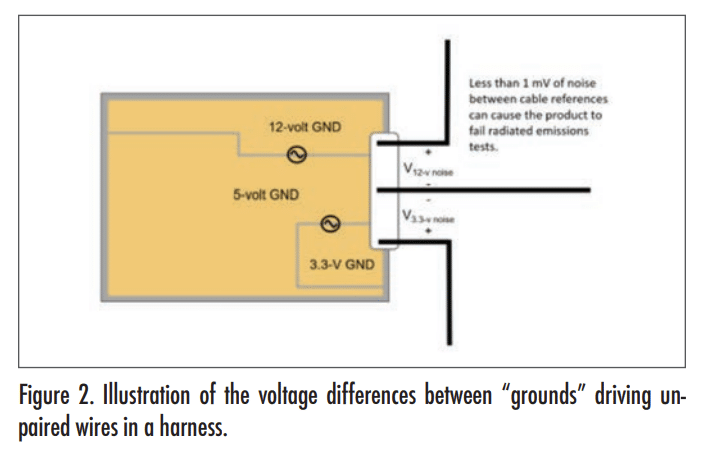
At frequencies where radiated emissions are likely to be a concern, a voltage as low as 1 mV between unpaired wires in a wiring harness can result in EMC test failures. [In some frequency bands, 0.1 mV is sufficient to cause a failure.] In order to ensure that a design complies with radiated emissions requirements (and for similar reasons, radiated immunity requirements), it is extremely important to maintain a single RF ground reference for every circuit connected to a wiring harness. Ensuring that all of the wires in a harness are held to the same potential (within 0.1 mV) at RF frequencies is relatively straightforward in a design with a single solid ground plane; but it can be extremely difficult in boards with isolated grounds.
Why Isolate Grounds?
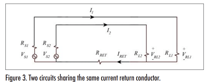
If isolating grounds is such a bad practice, why are so many boards designed that way? Often, the answer is that the designers were following the advice of a component supplier’s application note, or they were simply mimicking the design of a product that had been successful in the past. There is one valid reason that a board designer might not want to let two circuits share the same ground plane. That is to prevent common-impedance coupling. Common-impedance coupling (or conducted coupling) occurs when two circuits share parts of their current paths. Currents from the circuit behaving as the noise source flowing in the shared part induces a voltage in both circuits. For example the two circuits represented schematically in Figure 3 share the same current return path. The impedance of that return path is RRET. If Circuit 1 (the outer loop) creates a current, IRET, flowing in the return path, then a voltage is developed across the return path, VRET = IRET RRET. By Kirchhoff’s voltage law, some of this voltage will appear across the Circuit 2 source, and the rest will appear across the Circuit 2 load.
Common-impedance coupling is one of four EM coupling mechanisms, along with electric-field coupling, magnetic-field coupling and radiation coupling. Common-impedance coupling is most likely to be important at relatively low frequencies when the source circuits have relatively low impedance. The two most common methods for reducing common-impedance coupling are to reduce the impedance of the shared part of the circuit, or to isolate the circuits so that they don’t share a current path.
Providing separate “grounds” for various circuits on a circuit board is one method for reducing the common-impedance coupling between these circuits. This can be effective if high-current circuits use the ground plane as part of their current return path, and if that path is shared by circuits sensitive to small noise voltages. It is important to note that isolating current-return paths by partitioning a solid copper plane is only effective for reducing common-impedance coupling. The other EM coupling mechanisms are generally not affected by partitioning the return plane. In fact, gapping a solid ground plane can actually increase the electric and magnetic field coupling between traces routed over different portions of the plane.
When Should Current Returns be Isolated?
Designs that isolate current return conductors are justified when common-impedance coupling is a significant concern. Unlike high-frequency currents, low-frequency (e.g. below 100 kHz) currents flowing on a printed circuit plane will spread out. This means that all circuits that use a “ground” plane to return low-frequency currents share a portion of their current paths.
In these situations, it’s relatively easy to quantify the maximum possible common-impedance coupling. The maximum possible voltage coupled to a victim circuit is equal to the maximum resistance of the plane times the maximum current produced by the source circuit. For example, consider the two circuits illustrated in Figure 4. A 3.3- volt digital signal shares the same current return plane as an actuator signal that can switch from 0 amperes to 10 amperes in less than 1 microsecond. To calculate the maximum possible common-impedance coupling, we’ll assume that the traces are near each other and calculate the coupling that would occur if they both ran the entire length of the board.
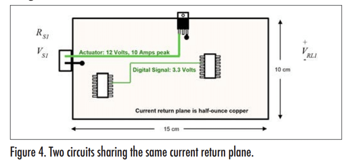
Since the plane is half-ounce copper (~17.8 µm thick), it has an end-to-end resistance of approximately,

Therefore, the maximum coupled voltage due to common-impedance coupling is,

Clearly, in this case, it is ok to allow these two signals to share the same current return plane. In fact, a few amperes of low-frequency current will generally translate to a few millivolts in a printed circuit board ground plane; so it is rarely necessary to provide an isolated return plane.
In rare situations where a calculation shows that low-frequency isolation is necessary, it is usually better to route the source or victim return currents on traces that occupy a different layer leaving the ground plane undivided. Generally, if two large grounds are isolated at low frequencies, they must still be connected at high frequencies in order to avoid radiated emissions and radiated immunity issues. Routing current returns on different layers facilitates their connection at high frequencies using capactors with low connection inductance.
The fact that the current switched in less than 1 microsecond was not a factor in this calculation. That’s because the dominant common impedance at low frequencies is the resistance of the plane. The coupled voltage waveform will mimic the shape of the source current waveform and the amount of common-impedance coupling will not depend on the rate of change of the signal. In the example above, electric-field and/or magnetic-field coupling would certainly be a significant concern. The field coupling would make it necessary to separate these traces. Nevertheless, it is critical to note that isolating the actuator’s return plane from the digital signal’s return plane would NOT significantly reduce the electric or magnetic field coupling.
Does Your Board Have Too Many Grounds?
It typically requires hundreds of millivolts of noise in order to interfere with digital logic. So unless the interfering circuits are switching hundreds of amperes of current, it is generally fine to allow these circuits to share a current return plane. Likewise digital logic, which typically switches peak currents on the order of hundreds of milliamps, can readily share a return plane with analog circuits capable of tolerating a few hundred microvolts of induced noise. Simple common-impedance coupling calculations like those in (1) and (2), will tell you if you need to isolate your current return paths at low frequencies.
At frequencies above 100 kHz, currents returning on a plane are concentrated beneath the signal trace. Common-impedance coupling is easily avoided by providing separation between the signal traces. Separating the traces is also generally effective for reducing electric and magnetic field coupling, which are much more likely to be the dominant coupling mechanisms at high frequencies.
A good rule of thumb when laying out automotive printed circuit boards is, “Never gap a solid ground plane.” In situations where it is necessary to isolate low-frequency return currents, route the return currents of either the source or the victim circuits on a different layer. This will make it easier to re-establish a connection between these “grounds” at high frequencies in order to meet radiated emissions and immunity requirements.
