INTRODUCTION TO SELF-GENERATED EMI
It seems many manufacturers these days are developing products that incorporate wireless technologies—both in new and existing products. Many of these products are using LTE cellular connectivity and designers are finding that the on-board DC-DC converters and processor/memory bus noise are creating enough broadband electromagnetic interference (EMI) that the cellular receiver downlink channels are being desensed (decreased sensitivity) to a point where the product is non-compliant with the cellular provider’s sensitivity requirements. Sometimes this broadband EMI even extends up to the GPS bands of 1575.42 MHz affecting navigational performance.
Cellular providers have strict receiver sensitivity requirements and the Total Isotropic Sensitivity (TIS) is one of the tests performed during CTIA compliance. If the receiver is not sensitive enough, the product will not be allowed onto the cellular system (References 1 and 2).
WHY PROPER PC BOARD DESIGN IS KEY
One factor that is always key to low-EMI designs is proper PC board design. If high-speed signals are not captured within transmission line structures, common mode current generation, EMI radiated leakage and crosstalk can result. Very often, I find clients use layer stack-up designs suggested in the 1990s for modern wireless designs of today and this is just asking for trouble, with associated schedule delays, debugging, and repeated compliance testing.
In order to understand why proper PC board design is a major key to success, let’s first understand how highspeed signals move in circuit boards.
HOW SIGNALS MOVE IN PC BOARDS
I suspect many of us were taught in university or college that electric current was the flow of electrons in copper wires or circuit traces, and that signals traveled at near the speed of light. This is inaccurate. It was also unlikely we were taught much about how signals propagated in circuit board transmission lines during our fields and waves class.
Before you can understand how signals propagate in PC boards, you must first understand some physics (References 3 and 4).
This current flow is partially true, of course, for DC circuits (with exception of the initial battery connection transient). But for AC (or RF) circuits or for the switching transients from switch mode power supplies, we need to understand all connecting wires/traces must now be considered transmission lines.
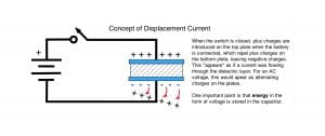
First, let’s consider how capacitors seemingly allow the “flow” of electrons. Referring to Figure 1, if we apply a battery to the capacitor, any positive charges applied to the top plate will repel positive charges on the bottom plate, leaving negative charges. If we apply an AC source to the capacitor, it might seem as if the current flows through the dielectric, which is impossible. James Clerk Maxwell called this “displacement current,” where positive charges merely displace positive charges on the opposite plate leaving negative charges, and vice versa. This displacement current is defined as dE/dt (changing E-field with time).
Electrons and the positively-charged holes do not travel at near light speed in copper as was implied, but move at about 1 cm/sec, due to the very tight atomic bond of the copper molecules (Reference 4). There are certainly clouds of free electrons and holes, but these move slowly from molecule to molecule. This is called conduction current and is what we would measure with an ammeter. Conduction current is related to the tangential component of the B-field, that is the curl B = J.
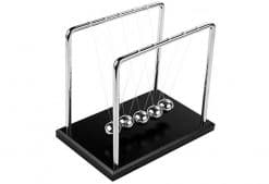
The influence of one electron in the copper molecule to its neighbor (and on down the transmission line) propagates at the speed of the electromagnetic (EM) field in the dielectric material. In other words, jiggle one electron at one end of a microstrip and it jiggles the next, which jiggles the next, and so on, until it jiggles the last one at the load end of the transmission line. This jiggling is called a kink in the E-field and can be envisioned as the Newton’s Cradle toy, a mechanical analogy, where the first ball hits the next and this eventually pops off the end ball (Figure 2).
Let’s now consider a digital signal with a wavefront moving at about half-light speed (about 6 in/ns in FR4 dielectric) along a simple microstrip over an adjacent ground return plane (GRP) as illustrated in Figure 3.
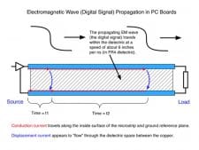
The next important point is that the EM field of the digital signal travels in the dielectric space—not the copper. The copper merely “guides” the EM wave (References 4 and 5).
When the signal (EM wave) is first applied between the microstrip and GRP, it starts to propagate along the transmission line formed by the microstrip over an adjacent GRP. There is a combination of conduction current and displacement current (across the dielectric). EMI harmonics originate at the wavefront as the EM wave propagates. The fast rise or fall times of the signal contain all the harmonic energy and this is what creates the EMI.
If the load impedance is equal to the characteristic impedance of the transmission line, then there will be no reflections of the EM wave back to the source. However, if there is a mismatch, there will be reflected EM fields propagating back to the source. In reality, most realistic digital signals will have multiple reflections moving back and forth through the transmission line simultaneously. The transition zone (rise time or fall time) of these propagating waves will potentially produce EMI.
PHYSICS-BASED RULES FOR TRANSMISSION LINES
With a better understanding of how signals move in circuit boards, there are two very important principles when it comes to low EMI PC board design:
- Every signal and power trace (or plane) on a PC board should be considered a transmission line.
- Digital signal propagation in transmission lines is really the movement of electromagnetic fields in the space between the copper trace and GRP.
To construct a transmission line, you need two adjacent pieces of metal that capture or contain the field. Examples include a microstrip over an adjacent GRP or a stripline adjacent to a GRP or a power trace (or plane) adjacent to a GRP. Locating multiple signal layers between power and ground reference planes will lead to real EMI issues for fast signals.
IMPORTANT POINT #1 – In other words, every signal or power trace (routed power) must have an adjacent GRP and all power planes should have an adjacent GRP. Many products end up violating these two rules, with resulting EMI issues.
IMPORTANT POINT #2 – If you break the path of the conduction current in the GRP through a gap or slot, we start to get “leakage” of the signal EM field throughout the dielectric space, which leads to edge radiation from the board and cross-coupling to other circuits through via-to-via coupling. This also occurs when we pass a signal through multiple ground reference or power planes if there is no nearby return path adjacent stitching via or stitching capacitor (to connect GRP to power planes). This self-generated EMI can easily conductively couple or radiate into sensitive cellular receivers. Please refer to the video demo explaining why gaps in the GRP are a disaster for EMI (Reference 6).
Via penetration: Very often, signals need to be run from the top side to the bottom side (or interior-to-interior layers), relying on vias to get there. If you only need to pass from one side of a GRP to the other, there’s no issue, because the electromagnetic field of the signal is contained between a constant metallic transmission line along the entire path (Figure 4).

It’s only when you need to pass through multiple planes that many designs fail to provide a continuous return path for the electromagnetic wave as it travels through the dielectric space of the board (Figure 5).
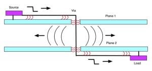
A lack of transmission-line continuity between the planes (using a stitching via or capacitor), will result in field leakage throughout the dielectric space as the signal tries to find a way back to the source. This field energy will couple to other vias, as well as propagate out as “edge radiation.”
If the two planes are GRPs, then you need to merely stitch them together in at least one location near the signal via. This allows field propagation along the entire path. A matrix of ground vias is always a good practice and if they’re located very close together (5 mm spacing is good), there’s no need to specifically locate one at each penetration.
A challenge presents itself when the two planes are at different potentials, such as a GRP and power, then a stitching capacitor needs to be installed next to the signal via. If there are dozens of signal penetrations on such a board, it may be impractical to add a stitching capacitor for every signal penetration, so that’s one reason to locate an even distribution of decoupling/stitching capacitors throughout the board. This will also help reduce “ground bounce” or simultaneous switching noise (SSN).
PROPER BOARD STACK-UP FOR LOW EMI
Observing these two important rules will dictate the layer stack-up. Following are some good and not so good EMI designs. More information on this topic may be found in References 7 and 8.
FOUR-LAYER BOARD: POOR (BUT TYPICAL) EXAMPLE
A typical four-layer board design I see often is (top to bottom): Signal – Ground Return Plane – Power Plane – Signal. This worked OK decades ago with relatively slow clock and signal frequencies, but is just asking for EMI issues in today’s high-frequency wireless technology. Let’s show a couple of four-layer examples that follow the rules. Note the lack of power planes.
FOUR-LAYER BOARD: GOOD DESIGN 1
Here is an example of a good four-layer board stack-up for improved EMI (Figure 6). Instead of a power plane, we use either routed or poured power, along with signals on layers 2 and 3. Thus, each signal/power trace is adjacent to a GRP. Also, it’s easy to run simple vias between all layers, so long as the two GRPs are also connected together with a matrix of stitching vias. If you run a row of stitching vias along the perimeter (say, every 5 mm) you form a Faraday cage. This is an excellent option for critical wireless products.

FOUR-LAYER BOARD: GOOD DESIGN 2
If, on the other hand, you’d prefer to have access to the signal and routed/poured power traces, you may simply reverse the layer pairs, such that the two GRP layers are in the middle and the two signal layers are positioned at the top and bottom, with routed power and sufficient decoupling caps, rather than a power plane (Figure 7).

For both four-layer designs, you want to run a 5-mm matrix pattern of stitching vias connecting the two GRPs.
For routed or poured power, every digital device will need 2-3 decoupling capacitors per power pin or tight groupings of pins. In addition, rails (typically the main digital voltages) should have wider pours around any high di/dt devices, such as core voltage, drivers, ASICs, motor controllers, processors, etc. This will help serve as your high frequency decoupling.
TYPICAL SIX-LAYER DESIGN: POOR EXAMPLE
One stack-up I frequently see is this six-layer design (Figure 8). This probably worked well enough in a decade or two ago, but like the poor four-layer design, it is a recipe for EMI disaster. There are two issues with this: the bottom two signal layers are referenced to the power plane and the power and ground return planes are non-adjacent and too far apart for best EMI decoupling.
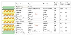
With few exceptions (some DDR RAM power and signals, for example) currents want to return to their sources, which are referenced to the GRP. Referencing these signals to the power plane is very EMI-risky, because there is no clearly defined return path, except through plane-to-plane capacitance, which in this case, is relatively small. In addition, the indefinite return path can result in field leakage into other areas of the board’s dielectric layers. That, in turn, leads to cross-coupling into wireless receivers and other circuitry and radiated EMI.
The second issue occurs when we have the power and GRP separated by two signal layers. Any power distribution network (PDN) transients will cross-couple to any signal traces on layers 3 and 4 within the dielectric layers. You also lose any plane-to-plane capacitance decoupling benefit if these planes are separated by more than 3-4 mils.
EIGHT-LAYER BOARD (GOOD EXAMPLE)
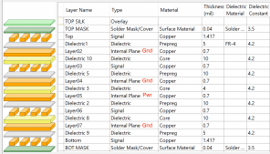
Both the four- and eight-layer board design examples (Figures 6, 7, and 9) follow the two fundamental rules (IMPORTANT POINT #1) that preserve good transmission line design and resulting low EMI. In addition, for the eight-layer design, the power and GRP planes are now 4 mils apart, providing good plane-to-plane capacitance. Closer spacing would be even better. For example, a spacing of 1 mil to 3 mils is ideal for minimizing EMI. Multiple GRPs should be stitched together with a 5-mm matrix pattern of vias.
Of course, there are many more iterations on creating proper transmission line pairs between signal and GRP or power and GRP.
PARTITIONING OF CIRCUIT FUNCTIONS
The next most important consideration when laying out the circuitry for your wireless board is partitioning of circuit functions, such as digital, analog, power conversion, RF, and motor control or other high-power circuits.
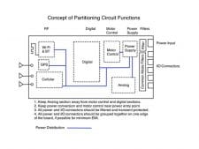
To avoid signal coupling and crosstalk, you must not allow the various return signals from intermixing within the same dielectric space. Thus, you need to partition major circuit functions. Figure 10 demonstrates one example of partitioning. Of course, this gets more challenging as board size shrinks. Henry Ott also describes this concept in Reference 9.
Another way to separate noisy circuits, such as digital and power conversion, from analog and RF circuitry, is to locate the digital on the bottom side of the stack-up and the analog and RF modules on the top side. For practical applications, this often assumes at least an eight-layer design with one, or more, GRPs near the middle to isolate the top and bottom sides. Great care must be taken to avoid coupling noisy circuitry with sensitive receivers, in the case of wireless designs.
Because low frequency (less than 50 kHz) or audio signal return currents tend to spread out more, that circuitry must be separated from digital, power conversion, or motor controller circuits. Likewise, sensitive RF receiver circuits, such as GPS, cellular, or Wi-Fi devices must also be kept separate from noisy digital, power conversion, or motor controller circuitry.
While Figure 10 implies routed power, it is very common to use 3.3V power planes under the digital circuitry for good EMI suppression. Power can also be routed as polygons under the appropriate circuit sections.
ADDITIONAL TIPS
Multiple ground vias: It’s a good practice to create a matrix of ground vias connecting GRPs together using a spacing of about 5-mm. This will provide multiple return paths for signals penetrating more than one GRP layer. In addition, if you use multiple GRPs, you should design via stitching all around the periphery of the board to create a Faraday cage for those signal layers in between. This technique is especially useful when incorporating wireless technology into the design.
Ground fills: While it seems to be a fairly common practice to fill in unused areas within each layer with ground fills, besides being unnecessary, they can lead to the issue of the “trace crossing a gap in the return” problem for dense boards where all the transmission line rules may be difficult to achieve. Eric Bogatin explains this a bit more in Reference 10.
Routed power versus power planes: The conventional method is to start with one or more (depending on the number of layers) power-ground “cores” and build the signal layers from there, usually equally on each side of the core for best manufacturability. Typically, digital ground return is used for this. Another big advantage is that when spaced very close together (less than 3 mils), the power-ground core becomes a good high-frequency decoupling capacitor. As the number of layers increase, it’s often best to locate two or more power-ground cores closer to the top and bottom of the stack-up — generally on layers 2-3 and 6-7 (on eight-layer boards, for example).
CONCLUSION
Most wireless products, especially smaller portable/mobile devices, now require greater care in their overall system design. An important key to low EMI and consequently, optimum performance, is the design of the PC board. You can largely “throw out” the layout rules used in past years, because at the clock and signal speeds used today, all copper traces become transmission lines and require more care to avoid gaps in the signal path where the electromagnetic wave can “leak out” and couple to sensitive circuits.
The important points to remember are that all signal and power networks should now be considered as transmission lines, the signals and power transients travel at about half-light speed within the dielectric space, the copper traces “guide” the signals along the GRP, and circuit functions need to be partitioned across the board real estate in order to reduce coupling. Maintaining these guidelines will help assure the lowest EMI and best performing wireless designs.
REFERENCES
- CTIA, Test Plan for Mobile Station Over the Air Performance: Method of Measurement for Radiated RF Power and Receiver Performance, http://files. ctia.org/pdf/CTIA_OTA_Test_Plan_Rev_3.1.pdf
- Broadcom, Compliance with TIS and TRP Requirements, https://www.broadcom.com/collateral/ wp/21XX-WP100-R.pdf
- Schmitt, Electromagnetics Explained – A Handbook for Wireless/RF, EMC, and High Speed Electronics, Newnes, 2002.
- Bogatin, Signal Integrity – Simplified (3rd edition), Prentice Hall, 2018.
- Beeker, Effective PCB Design: Techniques To Improve Performance, https://www.nxp.com/filesstatic/training_pdf/WBNR_PCBDESIGN.pdf
- Wyatt, Gaps in Return Planes (video), https://www. youtube.com/watch?v=L44lTnQgv-o&t=9s
- Hartley, Control of Noise, EMI and Signal Integrity in PC Boards (2-day seminar), Rick Hartley Enterprises, managed by https://www.pcb2day.com.
- Morrison, Fast Circuit Boards – Energy Management, Wiley, 2018.
- Ott, Electromagnetic Compatibility Engineering, Wiley, 2009.
- Bogatin, Seven Habits of Successful 2-Layer Board Designers (Signal Integrity Journal), https://www. signalintegrityjournal.com/blogs/12-fundamentals/ post/1207-seven-habits-of-successful-2-layerboard-designers
