Introduction
A very useful tool for troubleshooting EMC issues is the near field probe. Due to its small size (compared against antennas) the most common use of these tools is to aid in detection of the source of a particular signal (emission), or as a local field-generating source (immunity), helping you to find weak spots in your device under test. There are several options available costing from hundreds up to thousands of dollars. In this article, I will show you how to build your own set of near field probes for a few bucks and a cheap pre-amplifier enabling you to get started troubleshooting EMC issues.
My probes
I have been making my own EMC gear for a while, so last year I built two H-field probes (red ones on figure 1). I also have an extra probe (unshielded) which was a gift from a lab technician. He built it in a fashion to comply with a certain standard that I am not aware of (so I am probably not making the best use of it!). It has a lot of external interference for emissions (due to poor shielding) but it is quite effective for immunity testing.
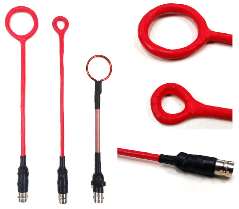
Figure 1 – H-field probes. At right details of the ones that I made myself.
I followed the article “Probing the magnetic probe” from Roy Ediss [1] to make what he calls a “King type with central gap” probe. The basic idea is to create a closed loop on a coax cable and cut a single slot in the outer sheath (gap). You can find other designs in his article that are even easier to make and the main difference between them is their self-resonating frequency, which will vary according to the parasitic capacitances and inductances of the probe, which depends on how you build it (among other things).
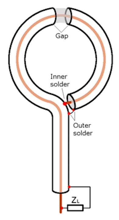
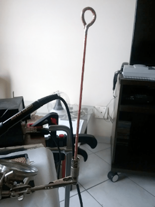
Figure 2 – a) H-field probe based on Roy Ediss’ design b) Making my own probe at home.
To make the probe I got a regular 50Ω coax cable with rigid center conductor that I had on hand, removed the outer jacket, the foil and braided shield, and wrapped a copper tape around the dielectric to replace the braid. I am not sure if this would significantly change the probe characteristic impedance but replacing the braid by the copper tape made it very easy to solder, cut the small gap and keep it rigid. It may be a good idea to replace the flexible coax cable by a semi-rigid one, but they are not so easy to find.
To build the loop you have to solder the inner conductor in the tip to the outer sheath (inner solder on figure 2) and then the outer sheath in the tip to itself (outer solder on figure 2). Cut a slice of the outer sheath to make the gap in the center of the loop. It is important to keep the gap small (around millimeter). After that, I soldered the inner conductor on the base to one end of a BNC adapter (double female), two 100Ω SMD resistors between BNC adapter’s inner and outer conductors diametrically opposed and finally the shielding copper tape to the outside of the BNC. Then I acquired a can of red liquid electrical tape and applied some coats of it to the entire thing until I got a thick wall and an even finish. For the smaller one I could simply dip the tip into the can. Finally, I placed a shrinkable sleeve between probe and BNC connector. As an alternative, you can skip the outer solder and the gap cutting, leaving only the inner solder done and you will have another probe design (not the “King type with central gap”).
On one occasion, I had access to a Beehive Electronics’ probe set (very nice stuff if you can afford it) and did some quick comparison between them and my probes and, for my surprise, they have a quite similar sensitivity. Of course, my test setup was not reproducible enough to compare the readings numerically, but at least I could see similar emission patterns as shown on figure 3.
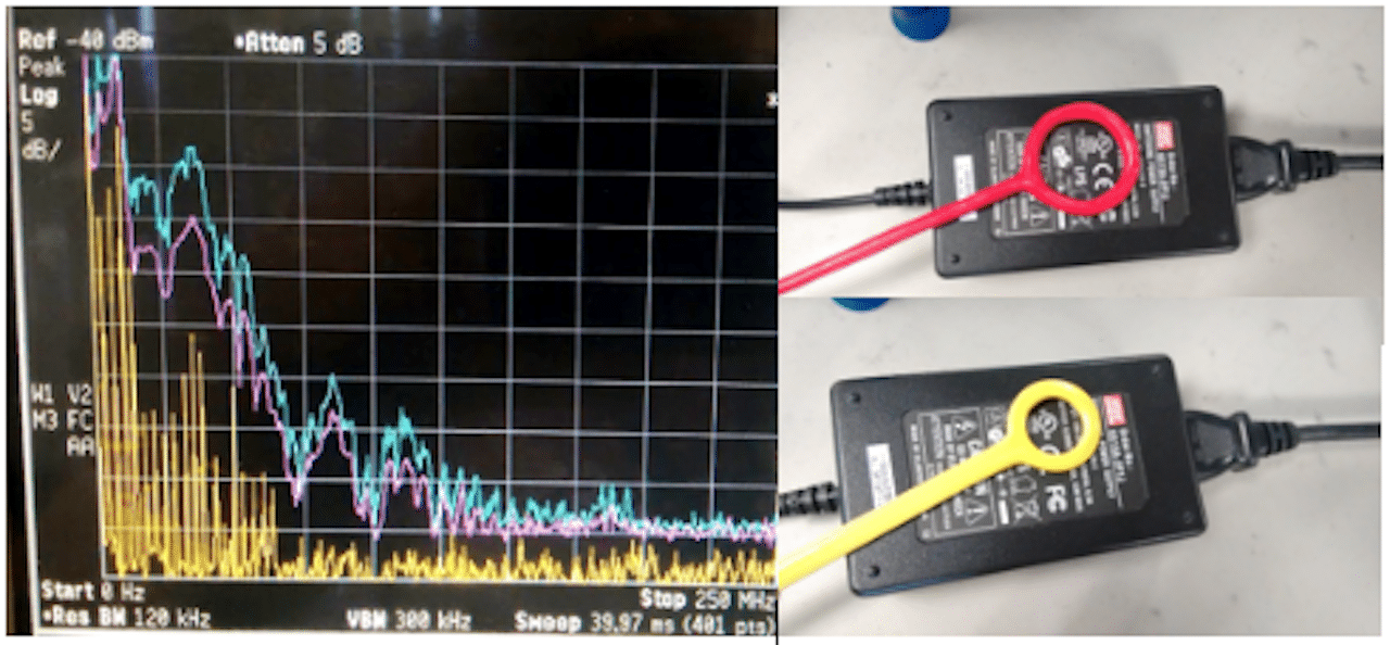
Figure 3 – Comparison between mine (pink trace) and Beehive’s probe (green trace)
Making a Tiny Probe
Since I often use near field probes for finding a source of magnetic field, it is helpful to have a probe that can find exactly the trace generating the unwanted emission. To achieve this resolution, you will need a probe with a tiny tip. I will show you how to build one based on Kenneth Wyatt’s course “EMC Troubleshooting and Pre-Compliance Testing for Product Designers” available on Fast Pass Online Training Hub [2].
To do my own tiny probe, I got a spare Wi-Fi antenna used for an old project, which has a thin wire (probably RG316) and an SMA connector. I took the antenna apart and made three levels of cut to the coax cable like shown on figure 4 (1st cut: expose braid; 2nd cut: expose dielectric; 3rd cut: expose inner wire).


Figure 4 – a) Spare Wi-Fi antenna; b) Layers diagram; c) Coax with exposed layers
I put a little drop of solder to the end of the braid to hold it together for the next steps. After that, I soldered the inner wire to the braid creating a loop. The loop shape is around 5x2mm and it is not perfectly round because the braid solder made it rigid.
I thought it would be nicer if the cable was not too flexible for the probe to reach the inside of an equipment without bending, so I came out with an idea: I got a pair of 0.8mm steel wires and twisted them tight together with a drilling machine to get a nice straight rod. After that, I placed the rod along with the coax cable and squeezed all together with a shrinkable sleeve from the outside.
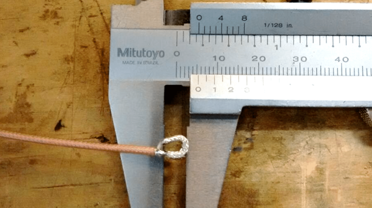
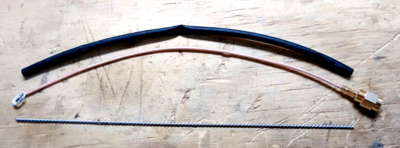
Figure 5 – a) Inner conductor soldered to braid forming a loop; b) Shrinkable sleeve, probe and twisted rod
After heating the sleeve, I dipped the tip into the can of liquid electrical tape. I really liked the finishing and, of course, I like the fact that the probe works just fine! One day after and the coating was completely dry and shrunk a little, exposing details of the inner shape.

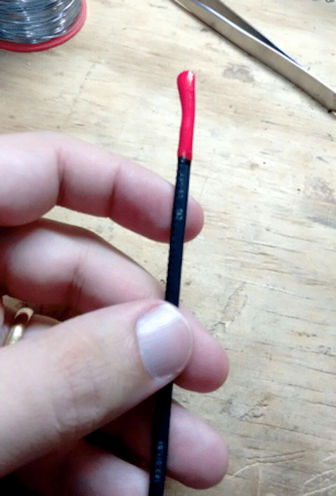
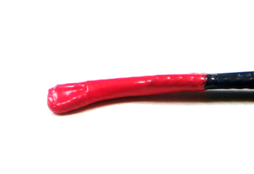
Figure 6 – a) Finished probe; b) Right after applying insulation coating; c) Coating in the day after
Low Noise Preamplifier
It is handy to have a preamplifier to amplify the signal of your freshly made H-field probes. I have a low noise amplifier (LNA) module from Mini-Circuits model ZX60-3018G+ [3] that is very helpful in finding small signals (especially if you are using the tiny probe). I like to build stuff, so I’ve got a chunk of aluminum and made myself a shiny base to place a connector, switch and LED to seat my amplifier on (after a lot of filing and sanding). Despite being a simple project, I am very proud on how it came out. The amplifier can be powered by battery or any DC supply through the power jack.
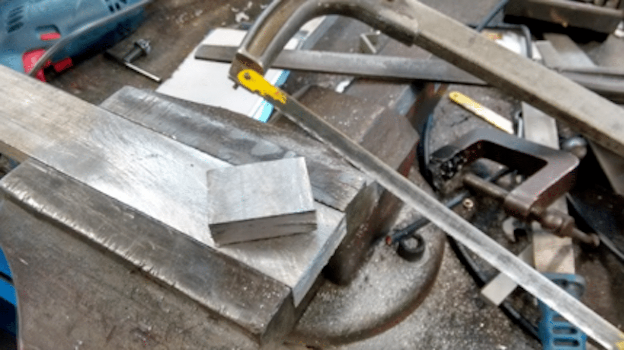
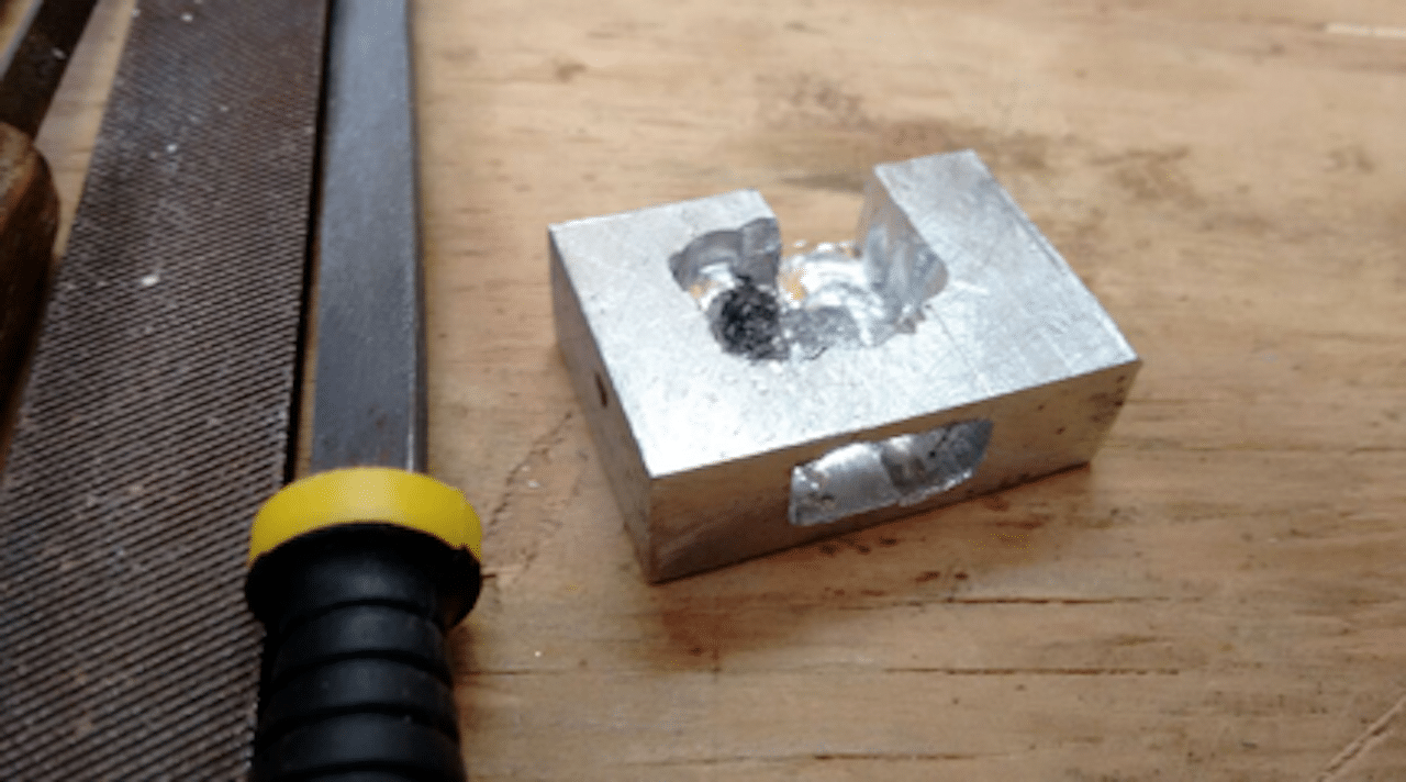
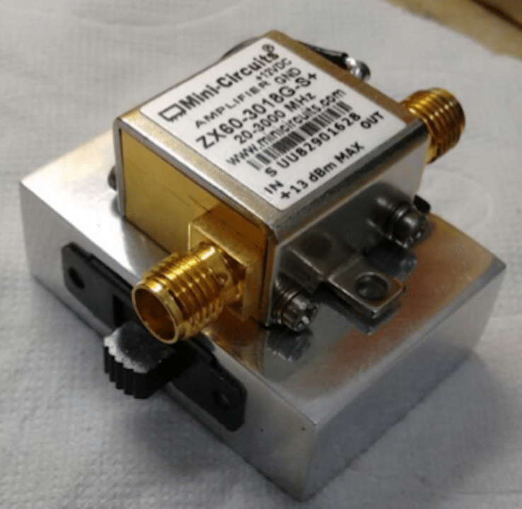
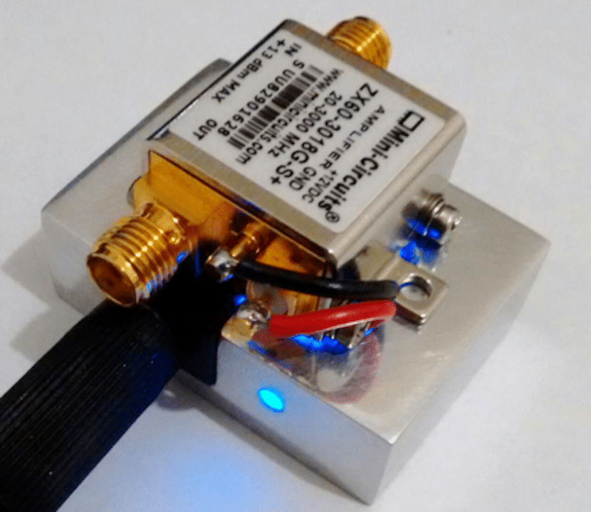
Figure 7 – Making the amplifier: from the aluminum chunk to the shiny assembly
Another cheap solution that I tested (and works very well) is the LNA4ALL from 9A4QV based on Mini-Circuits part number PSA4-5043+ [4]. Even CATV amplifiers can do a good boost to your signals but it will be a little noisier. A good practice is to know your environment when using near field probes outside a shielded room or when using a noisy amplifier: always check if the emission spikes you are looking at remain visible when you move the probes away from the device under test.
Summary
If you, just like myself, don’t have a large budget or live in a place where it is difficult to buy equipment for troubleshooting your EMC issues, you would only need a couple bucks or maybe recycle parts from old projects and a few hours to make your own near field probes. Even if you already have a set of probes, learning how to make near field probes can be useful to create custom probes if you need. You should now be able to get yourself a spectrum analyzer (or even a good oscilloscope), a bunch of wires and go outside exploring equipment RF emissions and troubleshooting some (or maybe most) EMC test issues!
References
[1] Probing the magnetic field probe by Roy Ediss http://www.ediss-electric.com/general_pdf/Probing_the_mag_field_probe.pdf
[2] Access the online course EMC Troubleshooting and Pre-Compliance Testing for Product Designers at https://emcfastpass.com/training/index.php/course/emc-troubleshooting/
[3] Find this amplifier and more RF circuits at https://www.minicircuits.com/
[4] Purchase LNA4ALL and find more information at http://lna4all.blogspot.com


