Introduction
The rapid development of the automotive industry and the trend towards autonomous vehicles and ADAS systems continue to drive the need for more sophisticated EMC design and test scenarios for the automotive industry. Vehicle platforms become increasingly much more complex with electronic devices that need a reliable function without impacting security or communication infrastructure.
The increase of electronics in automotive systems has not just foreseen a radical change in control systems with ECUs, but also in the communication, information, security and mobile entertainment systems in vehicles. It is important that all the electronic devices of a vehicle are electromagnetically compatible and do not interfere with the systems outboard.
The new wireless communication paradigms applied to the automotive sector require high performance electronic systems that operate at high bitrates and, therefore, at high frequencies according to the operating environment. Each of these new sub-systems must comply with the electromagnetic compatibility (EMC) standards. Furthermore, the integrity of the signals, the transmitted and processed data streams are critical aspects. Miniaturization of electronic products is a must and, as a consequence, manufacturing tolerance can be no longer neglected. Variations in nominal design parameters cause irregular behaviours that negatively affect the EMC and signal integrity and power (SI / PI) aspects.
Signal Integrity
Historically, engineers have used signal integrity testing (SI) as a key part of design and development of new systems and for maintaining standard qualifications. With today’s increasing demand for higher system throughput and reduced latency in cloud computing, customers are increasingly designing low-loss laminate materials with more stringent design specifications and tolerances for impedance control.
The integrity analysis continues to evolve by combining simulation models with instrumentation to include detailed measurements of non-uniform trace structures, vias, packages and connectors. As the PCBs become more complex, the lines between the different scopes of analysis become blurred. The concepts of signal and power integrity are closely related. Power integrity problems in a project can actually appear as signal integrity problems. That’s why performing signal integrity analysis is important for creating reliable designs, as well as for understanding and resolving possible problems encountered in the laboratory.
Digital projects traditionally have not been suffered of problems associated with the loss of a transmission line that can have significant consequences on the transmitted data. At low speeds, the frequency response has low influence on the signal. However, as speed increases, high frequency effects take over and even shorter lines can suffer of interferences such as crosstalk and reflections. In this case, the characteristics of a circuit can be determined as a function of parasitic impedances, which become prevalent along a transmission line

Figure 1: circuit model of a transmission line (on the left) and approximation to the first order (on the right)
An example of circuit model is shown in figure 1. The impedance plays an important role determining a perfect match of the transmission path of the signal and therefore effects on the quality of the signal. A mismatching between the line, source and load impedances determines a reflection of the signal with consequent energy loss and signal degradation. At high data rates this can cause overshoot of the signal, undershoot and stepped waveforms, which produce signal errors.
The mismatch of impedance can be overcome through the use of circuit schemes with simple parallel (see Figure 2) and more complex RC terminations in which a resistor-capacitor network provides a low-pass filter to remove low-frequency effects but passes the high-frequency signal.
 Figure 2: parallel termination circuit diagram
Losses in the high frequency signal transmission line make difficult for the receiver to interpret the information correctly. The following two causes of losses in a transmission line are due to the transmission medium:
■ Dielectric absorption: high frequency signals excite the molecules in the insulation, reducing signal level. Dielectric absorption refers to the PCB material.
■ Skin effect: high frequency signal current tends to travel on the conductors with an increase in the self-inductance of the material. The effective reduction of the conductive material causes an increase in resistance and, therefore, the attenuation of the signal (figure 3). The density of alternating current J in a conductor decreases exponentially from its value on the surface Js according to depth d from the surface:

Where ρ is the resistivity of the conductor, ω is the angular frequency, μ is the magnetic permeability, ε is the permittivity of the material.
 Figure 3: PCB section. The current route is orange. In blue is the ground plane and in celestial is the dielectric of the material. The copper PCB trace is highlighted in black.
CMOS circuits are very popular in many automotive sectors, due to their high speed and very low power dissipation. An ideal CMOS circuit dissipates energy only when it changes state and when the capabilities of the node need to be charged or discharged. In general, a CMOS requires an average of 10 mA and emission limitation techniques are focused on peak voltage and current values rather than average.
The rising current from the power supply on the chips pin is a primary source of emission. By placing a bypass capacitor near each power pin, this problem is limited. Larger capacitors provide strong current peaks, and tend to react badly to high-speed demands. Very small capacitors can react quickly to demand, but their total charge capacity is limited and can quickly run out. The best solution for most circuits is a mix of different sizes of parallel capacitors, perhaps 1-μF and 0.01-μF in parallel.
One area in which automotive designers are interested is in the AM radio band. Most every car is equipped with radios, which has a very sensitive and high gain tuneable amplifier from 500 kHz to 1.5 MHz. Many switching power supplies use switching frequencies within this same band, which leads to problems in automotive applications. As a result, most devices use switching frequencies above this band, often at 2 MHz or higher.
Automotive standard
The automotive industry and the car manufacturers have the aim of satisfying a variety of requirements regarding electromagnetic compatibility (EMC). For example, two requirements must ensure that electronic devices do not emit excessive electromagnetic interference (EMI) or noise and are immune to noise emitted by other systems.
Automotive systems have several receivers installed around the car. The IEC Commission has formulated international standards to protect them. The international standard for this electromagnetic noise is formulated as CISPR 25, and the power supply on board is required to meet this standard (figure 4).

Figure 4: electromagnetic noise
Automotive standards that relate to electromagnetic compatibility (EMC) are mainly developed by CISPR, ISO and SAE. CISPR and ISO are organizations that develop and maintain standards for international use. The CISPR 25 and ISO 11452-2 standards form the basis of most other standards.
CISPR 25 is a standard with different test methods. It requires that the level of test electromagnetic noise is being performed is at least 6 dB lower than the lowest measured levels. Another standard of testing is the ISO 11452-4 Bulk Current Injection (BCI) to check if a component is negatively affected by the narrow band electromagnetic fields. The test is performed by coupling noise directly in the wiring with a current probe.
CISPR 25 contains limits and procedures for measuring radio interference in the frequency range from 150 kHz to 1000 MHz. The standard applies to any electronic / electrical component intended for use on vehicles, trailers and devices. CISPR 25 defines the test configuration as shown in Figure 5 for measuring the noise of the radiation emitted by the apparatus.

Figure 5: EMI Radiated Noise Test Configuration Example
In the case of irradiated noise measurement of 1 GHz or less, the antenna is placed in the middle of the harness. The wiring current (or voltage) (or LISN) is measured for the conducted noise. The length of the line is different from the test condition for the radiation noise. Therefore, it is important to reduce the noise source level and to prevent noise propagation along the line to reduce EMI noise.
EMC Testing
When a magnetic field is present, a coil of conductive material can act as an antenna and convert the magnetic field into a current flowing around the wire. The small size of these loops minimizes the inductive effects of these materials. An example of this effect is when there is a differential data signal. A loop can be formed between the transmitter and the receiver with the differential lines. Another common loop is when two subsystems share a circuit, for example a display and an ECU device.
When a high-speed signal is sent through a transmission line and encounters a change in the characteristic impedance, part of the signal is reflected back and the other continues along the electrical path. Then, reflection leads to emissions.
Emissions can be caused by an interruption in the signal track or in the ground plane. For this it is necessary to avoid sharp angles on the signal track. To minimize reflections on components, it’s important to use small components such as size 0402 and set the width of the track equal to the width of the 0402 component.
A recurring topic when trying to solve EMI problems is to reduce dv/dt or di/dt where possible. In this context, DC-DC converters may seem completely harmless until switching regulators are much more efficient than other linear solutions. One area in which automotive designers are interested in creating interference is in the AM radio band. The cars are equipped with AM solutions, which have a very sensitive and high-gain tuneable amplifier from 500 kHz to 1.5 MHz. Most automotive switching supplies use the switching frequencies above this band, often at 2 MHz or higher. If the filter is not sufficient to contain this interference, it can trigger an EMI cycle over the whole circuit.
There are several ways to implement EMI noise reduction countermeasures.
Spread Spectrum Clock Generation (SSCG) is a method by which the energy contained in the small band of a clock source is spread on a larger one in a controlled mode, thus reducing the spectral amplitude of the fundamental and harmonics to reduce the emission radiated by the clock. This is obtained by modulating the clock frequency with unique shapes that allow reaching the peak of reduction of the EMI.
By varying the clock frequency on a band in a controlled mode, the time elapsed from the signal at a certain frequency is reduced, and in this way the concentration of energy at any frequency is reduced. So energy is spread on the band of frequencies that reduce the amplitude of the peak.
SSCG provides a way to reach EMC goals. It is an active solution, preserves the integrity of the clock, and can cover a wide range of frequencies. Compared to traditional methods of using passive components such as ferrite beads, RF coils to suppress EMI, SSCG uses an integrated circuit of active components to reduce the EMI peak using frequency modulation (Figure 6).
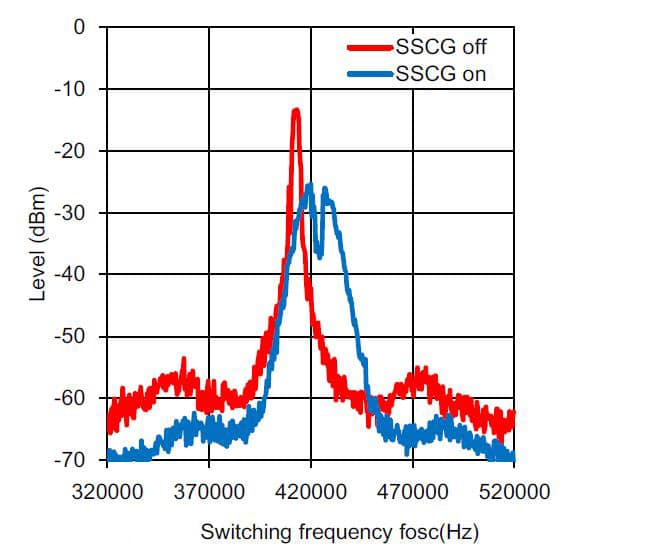
Figure 6: EMI reduction with SSCG
Power circuits
Various electronic devices are mounted on vehicles with different power sources. Switching circuits help power management solutions but are essentially noise sources. Where it is not possible to increase the switching frequency is necessary to introduce noise suppression measures.
DC-DC switching solutions for automotive systems have a switching frequency of 2 MHz, with the exception of some devices. Therefore, there is almost no problem in the range of AM radio (from 530 kHz to 1.8 MHz) as it is below 2 MHz, but countermeasures could be requested with values above 2 MHz. In particular, high noise frequency above 30 MHz is the most important since it generates cases of interference such as to interrupt the correct functioning of a system. A diagram of the step-down DC-DC converter is shown in the following figure 7.

Figure 7: step-down converter with current loop in various cases depending on the switch position
The parasitic inductance of the loop generates a high frequency voltage and therefore noise. To reduce this high frequency, it is necessary to reduce the parasitic inductance and to improve the switching response speed. Noise suppression measures are not limited to vehicles and can also be used with other industrial equipment (Figures 8 and 9).
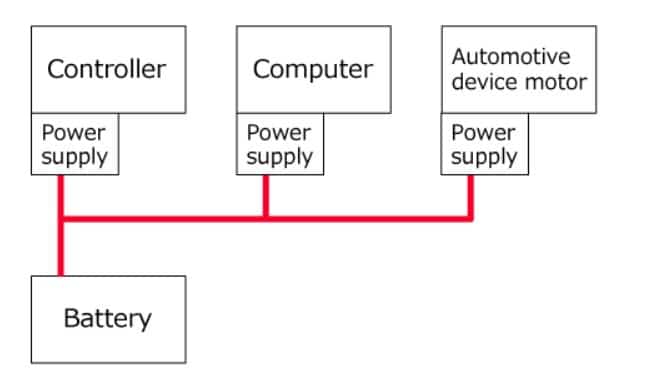
Figure 8: automotive power system
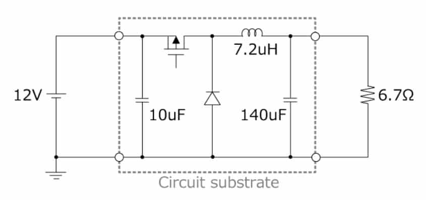 Figure 9: model of IC DC-DC step-down
Some methods consist of using appropriate shields to suppress noise up to 20 MHz. Or insert a common mode stop coil (CMCC) immediately next to the power connector to suppress noise in common mode at 20 MHz or higher, or, an LPF near the power connector to suppress noise in normal mode at 20 MHz or higher. In Figure 10 an implementation circuit of what has been described.
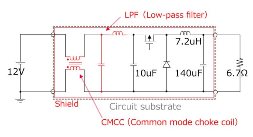
Figure 10: the circuit model of Figure 9 with noise suppression methods
Conclusion
Automobiles rely more on electronics: ADAS systems and self-driving vehicles; in all these there is a growing need to operate without errors without interfering with other systems in the vehicle. Through a selection of the appropriate components, materials and PCB study; engineers are able to design robust systems that enable automotive systems to operate EMI-free reliability.
